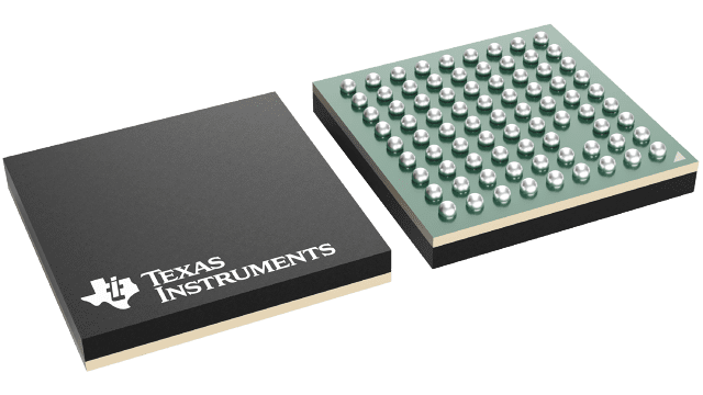
Información de empaque
| Encapsulado | Pines NFBGA (ZXH) | 80 |
| Rango de temperatura de funcionamiento (℃) -40 to 85 |
| Cant. de paquetes | Transportador 2,500 | LARGE T&R |
Características para SN65LVDS301
- FlatLink™3G serial interface technology
- Compatible with FlatLink3G receivers such as SN65LVDS302
- Input supports 24-bit RGB video mode interface
- 24-Bit RGB data, 3 control bits, 1 parity bit and 2 reserved bits transmitted over 1, 2 or 3 differential lines
- SubLVDS differential voltage levels
- Effective data throughput up to 1755 Mbps
- Three operating modes to conserve power
- Active-mode QVGA 17.4 mW (typ)
- Active-mode VGA 28.8 mW (typ)
- Shutdown mode 0.5 µA (typ)
- Standby mode 0.5 µA (typ)
- Bus swap for increased PCB layout flexibility
- 1.8-V supply voltage
- ESD rating > 2 kV (HBM)
- Pixel clock range of 4 MHz–65 MHz
- Failsafe on all CMOS inputs
- Packaging: 80 pin 5mm × 5mm nFBGA
- Very low EMI meets SAE J1752/3 ’M’-spec
Descripción de SN65LVDS301
The SN65LVDS301 serializer device converts 27 parallel data inputs to 1, 2, or 3 Sub Low-Voltage Differential Signaling (SubLVDS) serial outputs. It loads a shift register with 24 pixel bits and 3 control bits from the parallel CMOS input interface. In addition to the 27 data bits, the device adds a parity bit and two reserved bits into a 30-bit data word. Each word is latched into the device by the pixel clock (PCLK). The parity bit (odd parity) allows a receiver to detect single bit errors. The serial shift register is uploaded at 30, 15, or 10 times the pixel-clock data rate depending on the number of serial links used. A copy of the pixel clock is output on a separate differential output.
FPC cabling typically interconnects the SN65LVDS301 with the display. Compared to parallel signaling, the LVDS301 outputs significantly reduce the EMI of the interconnect by over 20 dB. The electromagnetic emission of the device itself is very low and meets the meets SAE J1752/3 ’M’-spec. (see Figure 6-22)
The SN65LVDS301 is characterized for operation over ambient air temperatures of –40°C to 85°C. All CMOS inputs offer failsafe features to protect them from damage during power-up and to avoid current flow into the device inputs during power-up. An input voltage of up to 2.165 V can be applied to all CMOS inputs while VDD is between 0V and 1.65V.