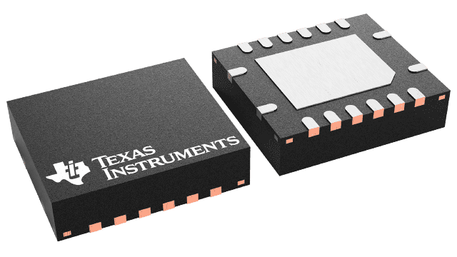
패키징 정보
| 패키지 | 핀 VQFN (RGY) | 16 |
| 작동 온도 범위(°C) -40 to 85 |
| 패키지 수량 | 캐리어 3,000 | LARGE T&R |
TS3V330의 주요 특징
- Low Differential Gain and Phase (DG = 0.82%, DP = 0.1 Degree Typ)
- Wide Bandwidth (BW = 300 MHz Min)
- Low Crosstalk (XTALK = -80 dB Typ)
- Low Power Consumption (ICC = 10 µA Max)
- Bidirectional Data Flow With Near-Zero Propagation Delay
- Low ON-State Resistance (ron = 3
 Typ)
Typ) - Rail-to-Rail Switching on Data I/O Ports (0 to VCC)
- VCC Operating Range From 3 V to 3.6 V
- Ioff Supports Partial-Power-Down Mode Operation
- Data and Control Inputs Provide Undershoot Clamp Diode
- Latch-Up Performance Exceeds 100 mA Per JESD 78, Class II
- ESD Performance Tested Per JESD 22
- 2000-V Human-Body Model (A114-B, Class II)
- 1000-V Charged-Device Model (C101)
- Suitable for Both RGB and Composite-Video Switching
TS3V330에 대한 설명
The TS3V330 video switch is a 4-bit 1-of-2 multiplexer/demultiplexer, with a single switch-enable (EN) input. When EN is low, the switch is enabled and the D port is connected to the S port. When EN is high, the switch is disabled and the high-impedance state exists between the D and S ports. The select (IN) input controls the data path of the multiplexer/demultiplexer.
Low differential gain and phase make this switch ideal for composite and RGB video applications. This device has wide bandwidth and low crosstalk, making it suitable for high-frequency applications as well.
This device is fully specified for partial-power-down applications using Ioff. The Ioff feature ensures that damaging current will not backflow through the device when it is powered down. This switch maintains isolation during power off.
To ensure the high-impedance state during power up or power down, EN should be tied to VCC through a pullup resistor; the minimum value of the resistor is determined by the current-sinking capability of the driver.
