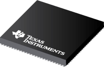
封裝資訊
| 封裝 | 引腳 NFBGA (ZCN) | 491 |
| 作業溫度範圍 (°C) -40 to 105 |
| 包裝數量 | 運送包裝 90 | JEDEC TRAY (5+1) |
AM3505 的特色
- AM3517/05 Sitara Processor:
- MPU Subsystem
- 600-MHz Sitara ARM Cortex-A8 Core
- NEON SIMD Coprocessor and Vector
Floating-Point (FP) Coprocessor
- Memory Interfaces:
- 166-MHz 16- and 32-Bit mDDR/DDR2
Interface with 1GB of Total Addressable
Space - Up to 83 MHz General-Purpose Memory
Interface Supporting 16-Bit-Wide
Multiplexed Address/DataBus - 64KB of SRAM
- 3 Removable Media Interfaces
[MMC/SD/SDIO]
- 166-MHz 16- and 32-Bit mDDR/DDR2
- IO Voltage:
- mDDR/DDR2 IOs: 1.8V
- Other IOs: 1.8V and 3.3V
- Core Voltage: 1.2V
- Commercial and Extended Temperature Grade
(operating restrictions apply) - 16-Bit Video Input Port Capable of
Capturing HD Video - HD Resolution Display Subsystem
- Serial Communication
- High-End CAN Controller
- 10/100 Mbit Ethernet MAC
- USB OTG Subsystem with Standard
DP/DM Interface [HS/FS/LS] - Multiport USB Host Subsystem [HS/FS/LS]
- 12-Pin ULPI or 6-, 4-, or 3-Pin Serial
Interface
- 12-Pin ULPI or 6-, 4-, or 3-Pin Serial
- Four Master and Slave Multichannel Serial
Port Interface(McSPI) Ports - Five Multichannel Buffered Serial Ports (McBSPs)
- 512-Byte Transmit and Receive Buffer
(McBSP1/3/4/5) - 5-KB Transmit and Receive Buffer (McBSP2)
- SIDETONE Core Support (McBSP2 and
McBSP3 Only)For Filter, Gain, and Mix
Operations - 128-Channel Transmit and Receive Mode
- Direct Interface to I2S and PCM Device and
TDM Buses
- 512-Byte Transmit and Receive Buffer
- HDQ/1-Wire Interface
- 4 UARTs (One with Infrared Data Association
[IrDA] and Consumer Infrared [CIR] Modes) - 3 Master and Slave High-Speed Inter-Integrated
Circuit (I2C) Controllers - Twelve 32-bit General-Purpose Timers
- One 32-bit Watchdog Timer
- One 32-bit 32-kHz Sync Timer
- Up to 186 General-Purpose I/O (GPIO) Pins
- MPU Subsystem
- Display Subsystem
- Parallel Digital Output
- Up to 24-Bit RGB
- Supports Up to 2 LCD Panels
- Support for Remote Frame Buffer Interface (RFBI)
LCD Panels - Two 10-Bit Digital-to-Analog Converters (DACs)
Supporting- Composite NTSC/PAL Video
- Luma/Chroma Separate Video (S-Video)
- Rotation of 90, 180, and 270 Degrees
- Resize Images From 1/4x to 8x
- Color Space Converter
- 8-Bit Alpha Blending
- Video Processing Front End (VPFE) 16-Bit Video Input Port
- RAW Data Interface
- 75-MHz Maximum Pixel Clock
- Supports REC656/CCIR656 Standard
- Supports YCbCr422 Format (8-Bit or 16-Bit with Discrete
Horizontal and Vertical Sync Signals) - Generates Optical Black Clamping Signals
- Built-in Digital Clamping and Black Level Compensation
- 10-Bit to 8-Bit A-law Compression Hardware
- Supports up to 16K Pixels (Image Size) in Horizontal
and Vertical Directions
- System Direct Memory Access (sDMA) Controller (32 Logical
Channels with Configurable Priority) - Comprehensive Power, Reset, and Clock Management
- ARM Cortex-A8 Memory Architecture
- ARMv7 Architecture
- In-Order, Dual-Issue, Superscalar Microprocessor Core
- ARM NEON Multimedia Architecture
- Over 2x Performance of ARMv6 SIMD
- Supports Both Integer and Floating-Point SIMD
- Jazelle RCT Execution Environment Architecture
- Dynamic Branch Prediction with Branch Target Address
Cache, Global History Buffer and 8-Entry Return Stack - Embedded Trace Macrocell [ETM] Support for
Noninvasive Debug - 16KB of Instruction Cache (4-Way Set-Associative)
- 16KB of Data Cache (4-Way Set-Associative)
- 256KB of L2 Cache
- ARMv7 Architecture
- PowerVR SGX Graphics Accelerator (AM3517 Only)
- Tile-Based Architecture Delivering up to 10 MPoly/sec
- Universal Scalable Shader Engine: Multi-threaded Engine
Incorporating Pixel and Vertex Shader Functionality - Industry Standard API Support: OpenGLES 1.1 and
2.0, OpenVG1.0 - Fine-Grained Task Switching, Load Balancing, and
Power Management - Programmable, High-Quality Image Anti-Aliasing
- Endianess
- ARM Instructions – Little Endian
- ARM Data – Configurable
- SDRC Memory Controller
- 16- and 32-Bit Memory Controller with 1GB of
Total Address Space - Double Data Rate (DDR2) SDRAM, Mobile Double Data Rate
(mDDR)SDRAM - SDRAM Memory Scheduler (SMS) and Rotation Engine
- 16- and 32-Bit Memory Controller with 1GB of
- General Purpose Memory Controller (GPMC)
- 16-Bit-Wide Multiplexed Address/Data Bus
- Up to 8 Chip-Select Pins with 128MB of Address
Space per Chip-Select Pin - Glueless Interface to NOR Flash, NAND Flash (with ECC
Hamming Code Calculation), SRAM and Pseudo-SRAM - Flexible Asynchronous Protocol Control for Interface
to Custom Logic (FPGA, CPLD, ASICs, and so forth) - Nonmultiplexed Address/Data Mode (Limited 2-KB
Address Space)
- Test Interfaces
- IEEE-1149.1 (JTAG) Boundary-Scan Compatible
- Embedded Trace Macro Interface (ETM)
- 65-nm CMOS Technology
- Packages:
- 491-Pin BGA (17 x 17, 0.65-mm Pitch)
[ZCN Suffix]
with Via Channel Array
Technology - 484-Pin PBGA (23 x 23, 1-mm Pitch)
[ZER Suffix]
- 491-Pin BGA (17 x 17, 0.65-mm Pitch)
AM3505 的說明
AM3517/05 is a high-performance ARM Cortex-A8 microprocessor with speeds up to 600 MHz. The device offers 3D graphics acceleration while also supporting numerous peripherals, including DDR2, CAN, EMAC, and USB OTG PHY that are well suited for industrial apllications.
The processor can support other applications, including: Single-board computers Home and industrial automation Human machine Interface
The device supports high-level operating systems (OSs), such as:
- Linux®
- Windows® CE
- Android™
The following subsystems are part of the device:
- Microprocessor unit (MPU) subsystem based on the ARM Cortex-A8 microprocessor
- PowerVR SGX graphics accelerator (AM3517 device only) subsystem for 3D graphics acceleration to support display and gaming effects
- Display subsystem with several features for multiple concurrent image manipulation, and a programmable interface supporting a wide variety of displays. The display subsystem also supports NTSC/PAL video out.
- High-performance interconnects provide high-bandwidth data transfers for multiple initiators to the internal and external memory controllers and to on-chip peripherals. The device also offers a comprehensive clock-management scheme.
AM3517/05 devices are available in a 491-pin BGA package and a 484-pin PBGA package.
This AM3517/05 data manual presents the electrical and mechanical specifications for the AM3517/05 Sitara processor.
