封裝資訊
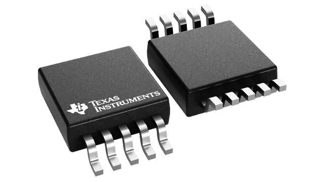
| 封裝 | 引腳 VSSOP (DGS) | 10 |
| 作業溫度範圍 (°C) -40 to 125 |
| 包裝數量 | 運送包裝 3,500 | LARGE T&R |
LM5060-Q1 的特色
- Available in Automotive Grade / AEC Q-100
- Wide operating input voltage range:
5.5 V to 65 V - Functional safety
capable
- Documentation available to aid functional safety system design
- Less than 15-µA quiescent current in disabled mode
- Controlled output rise time for safe connection of capacitive loads
- Charge pump gate driver for external N-Channel MOSFET
- Adjustable Undervoltage Lockout (UVLO) with hysteresis
- UVLO Serves as second enable input for systems requiring safety redundancy
- Programmable fault detection delay time
- MOSFET latched off after load fault is detected
- Active low open drain POWER GOOD (nPGD) output
- Adjustable input Overvoltage Protection (OVP)
- Immediate restart after overvoltage shutdown
- 10-Lead VSSOP
LM5060-Q1 的說明
The LM5060 high-side protection controller provides intelligent control of a high-side N-channel MOSFET during normal on/off transitions and fault conditions. In-rush current is controlled by the nearly constant rise time of the output voltage. A POWER GOOD output indicates when the output voltage reaches the input voltage and the MOSFET is fully on. Input UVLO (with hysteresis) is provided as well as programmable input OVP. An enable input provides remote on or off control. The programmable UVLO input can be used as second enable input for safety redundancy. A single capacitor programs the initial start-up VGS fault detection delay time, the transition VDS fault detection delay time, and the continuous over-current VDS fault detection delay time. When a detected fault condition persists longer than the allowed fault delay time, the MOSFET is latched off until either the enable input or the UVLO input is toggled low and then high.
