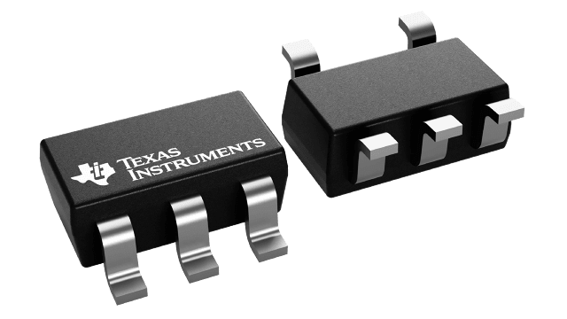
封裝資訊
| 封裝 | 引腳 SOT-23 (DBV) | 5 |
| 作業溫度範圍 (°C) -40 to 85 |
| 包裝數量 | 運送包裝 250 | SMALL T&R |
SN74AUP1G79 的特色
- Available in the Texas Instruments NanoStar™ Package
- Low Static-Power Consumption:
ICC = 0.9 µA Maximum - Low Dynamic-Power Consumption:
Cpd = 3 pF Typical at 3.3 V - Low Input Capacitance:
Ci = 1.5 pF Typical - Low Noise: Overshoot and Undershoot
< 10% of VCC - Ioff Supports Partial Power-Down-Mode Operation
- Input Hysteresis Allows Slow Input Transition and Better Switching Noise Immunity
at the Input
(Vhys = 250 mV Typical at 3.3 V) - Wide Operating VCC Range of 0.8 V to 3.6 V
- Optimized for 3.3-V Operation
- 3.6-V I/O Tolerant to Support Mixed-Mode Signal Operation
- tpd = 4 ns Maximum at 3.3 V
- Suitable for Point-to-Point Applications
- Latch-Up Performance Exceeds 100 mA Per JESD 78, Class II
- ESD Performance Tested Per JESD 22
- 2000-V Human-Body Model
(A114-B, Class II) - 1000-V Charged-Device Model (C101)
- 2000-V Human-Body Model
SN74AUP1G79 的說明
The AUP family is TI’s premier solution to the industry’s low-power needs in battery-powered portable applications. This family assures a very-low static and dynamic power consumption across the entire VCC range of 0.8 V to 3.6 V, thus resulting in an increased battery life. The AUP devices also maintain excellent signal integrity.
The SN74AUP1G79 is a single positive-edge-triggered D-type flip-flop. When data at the data (D) input meets the setup-time requirement, the data is transferred to the Q output on the positive-going edge of the clock pulse. Clock triggering occurs at a voltage level and is not directly related to the rise time of the clock pulse. Following the hold-time interval, data at the D input can be changed without affecting the levels at the outputs.
NanoStar™ package technology is a major breakthrough in IC packaging concepts, using the die as the package.
The SN74AUP1G79 device is fully specified for partial-power-down applications using Ioff. The Ioff circuitry disables the outputs when the device is powered down. This inhibits current backflow into the device which prevents damage to the device.
