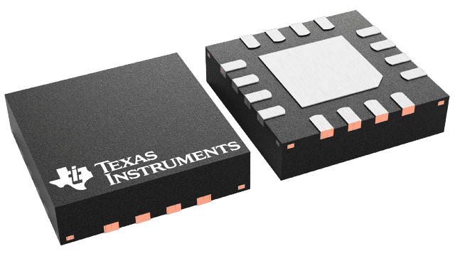
封裝資訊
| 封裝 | 引腳 VQFN (RGV) | 16 |
| 作業溫度範圍 (°C) -40 to 85 |
| 包裝數量 | 運送包裝 250 | SMALL T&R |
THS3217 的特色
- Input Stage: Internal Gain of 2-V/V
- Buffered Differential Inputs
- Single-Ended Low Impedance Output
- Full-Power Bandwidth: 500-MHz (2 VPP)
- Output Stage: Gain Externally Configurable
- Full-Power Bandwidth: 500-MHz (5 VPP)
- Slew Rate: 5000 V/µs
- SPDT Input Switch / Multiplexer
- Full Signal Path: Input Stage + Output Stage
- HD2 (20 MHz, 5 VPP to 100-Ω Load): –60 dBc
- HD3 (20 MHz, 5 VPP to 100-Ω Load): –75 dBc
- 10-VPP Output to 100-Ω Load Using Split
±6.5-V Supply - 12-VPP Output to Heavy Capacitive Loads Using Single 15-V Supply
- Internal DC Reference Buffer with Low Impedance Output
- Power-Supply Range:
- Split Supply: ±4 V to ±7.9 V
- Single Supply: 8 V to 15.8 V
THS3217 的說明
The THS3217 combines the key signal-chain components required to interface with a complementary-current output, digital-to-analog converter (DAC). The flexibility provided by this two-stage amplifier system delivers the low distortion, dc-coupled, differential to single-ended signal processing required by a wide range of systems. The input stage buffers the DAC resistive termination, and converts the signal from differential to single-ended with a fixed gain of 2 V/V. The differential to single-ended output is available externally for direct use, and can also be connected through an RLC filter or attenuator to the input of an internal output power stage (OPS). The wideband, current-feedback, output power stage provides all pins externally for flexible gain setting.
An internal 2×1 multiplexer (mux) to the output power stage noninverting input provides an easy means to select between the internal differential-to-single-ended stage (D2S) output or an external input.
An optional on-chip midsupply buffer provides a wideband, low-output-impedance source for biasing during single-supply operation through the signal-path stages. This feature provides very simple biasing for single-supply, ac-coupled applications operating up to a maximum 15.8-V supply. An external input to this buffer allows for a dc error-correction loop, or a simple output dc offset feature.
A companion device, the THS3215, provides the same functional features at lower quiescent power and bandwidth. The THS3217 and the THS3215 support the emerging high-speed Texas Instruments DACs for AWG applications, such as the DAC38J82.
