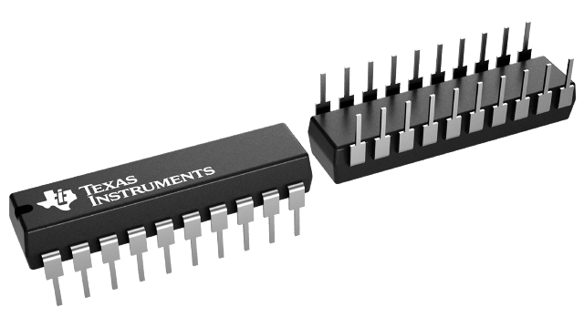
封裝資訊
| 封裝 | 引腳 PDIP (N) | 20 |
| 作業溫度範圍 (°C) -40 to 125 |
| 包裝數量 | 運送包裝 20 | TUBE |
TPIC6595 的特色
- Low rDS(on) . . . 1.3
 Typical
 - Avalanche Energy . . . 75 mJ
- Eight Power DMOS Transistor Outputs of 250-mA Continuous Current
- 1.5-A Pulsed Current Per Output
- Output Clamp Voltage at 45 V
- Devices Are Cascadable
- Low Power Consumption
TPIC6595 的說明
The TPIC6595 is a monolithic, high-voltage, high-current power 8-bit shift register designed for use in systems that require relatively high load power. The device contains a built-in voltage clamp on the outputs for inductive transient protection. Power driver applications include relays, solenoids, and other medium-current or high-voltage loads.
This device contains an 8-bit serial-in, parallel-out shift register that feeds an 8-bit D-type storage register. Data transfers through both the shift and storage registers on the rising edge of the shift-register clock (SRCK) and the register clock (RCK) respectively. The storage register transfers data to the output buffer when shift-register clear (SRCLR)\ is high. When SRCLR\ is low, the input shift register is cleared. When output enable (G)\ is held high, all data in the output buffers is held low and all drain outputs are off. When G\ is held low, data from the storage register is transparent to the output buffers. The serial output (SER OUT) allows for cascading of the data from the shift register to additional devices.
Outputs are low-side, open-drain DMOS transistors with output ratings of 45 V and 250-mA continuous sink current capability. When data in the output buffers is low, the DMOS-transistor outputs are off. When data is high, the DMOS-transistor outputs have sink current capability.
Separate power and logic level ground pins are provided to facilitate maximum system flexibility. Pins 1, 10, 11, and 20 are internally connected, and each pin must be externally connected to the power system ground in order to minimize parasitic inductance. A single-point connection between pin 19, logic ground (LGND), and pins 1, 10, 11, and 20, power grounds (PGND), must be externally made in a manner that reduces crosstalk between the logic and load circuits.
The TPIC6595 is characterized for operation over the operating case temperature range of -40°C to 125°C.
