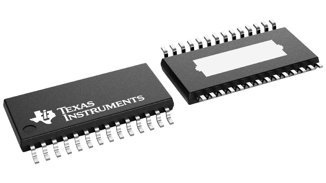
封裝資訊
| 封裝 | 引腳 HTSSOP (PWP) | 28 |
| 作業溫度範圍 (°C) |
| 包裝數量 | 運送包裝 50 | TUBE |
TPS56300 的特色
- 2.8 V – 5.5 V Input Voltage Range
- Programmable Dual Output Controller
Supports Popular DSP and Microcontroller
Core and I/O Voltages- Switching Regulator Controls Core
Voltage - Low Dropout Controller Regulates I/O
Voltage
- Switching Regulator Controls Core
- Programmable Slow-Start Ensures
Simultaneous Powerup of Both Outputs - Power Good Output Monitors Both Outputs
- Fast Ripple Regulator Reduces Bulk
Capacitance for Lower System Costs - ±1.5% Reference Voltage Tolerance
- Efficiencies Greater than 90%
- Overvoltage, Undervoltage, and Adjustable
Overcurrent Protection - Drives Low-Cost Logic Level N-Channel
MOSFETs Through Entire Input Voltage
Range - Evaluation Module TPS56300EVM-139
Available
PowerPAD is a trademark of Texas Instruments Incorporated.
TPS56300 的說明
The high performance TPS56300 synchronous-buck regulator provides two supply voltages to power the core and I/O of digital signal processors, such as the ‘C6000 family. The ripple regulator, using hysteretic control with droop compensation, is configured for the core voltage and features fast transient response time reducing output bulk capacitance.
The LDO controller drives an external N-channel power MOSFET and functions as an LDO regulator, suitable for powering the I/O or as a power distribution switch. To promote better system reliability during power up, voltage sequencing and protection are controlled such that the core and I/O power up together with the same slow-start voltage. At power down, the LDO and ripple regulator are discharged towards ground for added protection. The TPS56300 also includes inhibit, slowstart, and under-voltage lockout features to aide in controlling power sequencing. A tri-level voltage identification network (VID) sets both regulated voltages to any of 9 preset voltage pairs from 1.3 V to 3.3 V. Other voltages are possible by implementing an external voltage divider. Strong MOSFET drivers, with a typical peak current rating of 2-A sink and source are included on chip, enabling high system currents beyond 30 A. The high-side driver features a floating bootstrap driver with the internal bootstrap synchronous rectifier. Many protection features are incorporated within the device to ensure better system integrity. An open-drain output POWER GOOD status circuit monitors both output voltages, and is pulled low if either output fall below the threshold. An over current shutdown circuit protects the high-side power MOSFET against short-to-ground faults at load or the phase node, while over voltage protection turns off the output drivers and LDO controller if either output exceeds its threshold. Under voltage protection turns off the high-side and low-side MOSFET drivers and the LDO controller if either output is 25% below VREF. Lossless current-sensing is done by detecting the drain-source voltage drop across the high-side power MOSFET while it is conducting. The TPS56300 is fully compliant with TI DSP power requirements such as the ‘C6000 family.
