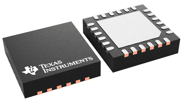
封裝資訊
| 封裝 | 引腳 VQFN (RGE) | 24 |
| 作業溫度範圍 (°C) -40 to 85 |
| 包裝數量 | 運送包裝 3,000 | LARGE T&R |
TPS65193 的特色
- Dual High-Voltage Scan Driver
- Scan Driver Output Charge Share
- High Output-Voltage Level: Up to 35 V
- Low Output-Voltage Level: Down to –28 V
- Logic-Level Inputs
- 24-Pin 4-mm × 4-mm QFN package
- APPLICATIONS
- TFT LCD Using Amorphous Silicon Gate (ASG) Technology
TPS65193 的說明
The TPS65193 is dual high-voltage scan driver to drive an amorphous-silicon-gate (ASG) circuit on TFT glass. Each single high-voltage scan driver receives logic-level inputs of CPVx and generates two high-voltage outputs of CKVx and CKVBx. The device receives a logic-level input of STV and generates a high-voltage output of STVP. These outputs are swings from Voff (–28 V) to Von (35 V) and are used to drive the ASG circuit and charge/discharge the capacitive loads of the TFT LCD. In order to reduce the power dissipation of the device, a charge-share function is implemented. The device features a discharge function, which shorts Voff to GND in order to shut down the panel faster when the LCD is turned off.
