SNAS378L November 2008 – February 2019 ADC14155QML-SP
PRODUCTION DATA.
- 1 Features
- 2 Applications
- 3 Description
- 4 Revision History
- 5 Pin Configuration and Functions
-
6 Specifications
- 6.1 Absolute Maximum Ratings
- 6.2 ESD Ratings
- 6.3 Recommended Operating Conditions
- 6.4 Thermal Information
- 6.5 ADC14155 Converter Electrical Characteristics DC Parameters
- 6.6 ADC14155 Converter Electrical Characteristics (Continued) DYNAMIC Parameters
- 6.7 ADC14155 Converter Electrical Characteristics (Continued) Logic and Power Supply Electrical Characteristics
- 6.8 ADC14155 Converter Electrical Characteristics (Continued) Timing and AC Characteristics
- 6.9 Timing Diagram
- 6.10 Transfer Characteristic
- 6.11 Typical Performance Characteristics, DNL, INL
- 6.12 Typical Performance Characteristics, Dynamic Performance
- 7 Detailed Description
- 8 Application and Implementation
- 9 Power Supply Recommendations
- 10Layout
- 11Device and Documentation Support
- 12Mechanical, Packaging, and Orderable Information
Package Options
Refer to the PDF data sheet for device specific package drawings
Mechanical Data (Package|Pins)
- NBA|48
Thermal pad, mechanical data (Package|Pins)
Orderable Information
7.3.1.1 Differential Analog Input Pins
The ADC14155QML-SP has one pair of analog signal input pins, VIN+ and VIN–, which form a differential input pair. The input signal, VIN, is defined as
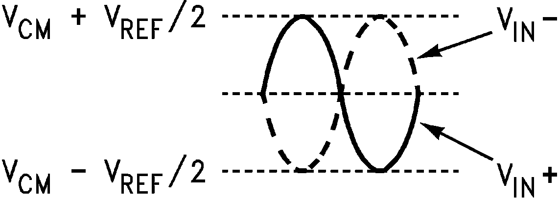
Figure 21 shows the expected input signal range. Note that the common mode input voltage, VCM, should be 1.5 V. Using VRM (pin 46 or 47) for VCM will ensure the proper input common mode level for the analog input signal. The peaks of the individual input signals should each never exceed 2.6 V. Each analog input pin of the differential pair should have a peak-to-peak voltage equal to the reference voltage, VREF, be 180° out of phase with each other and be centered around VCM.The peak-to-peak voltage swing at each analog input pin should not exceed the value of the reference voltage or the output data will be clipped.
 Figure 21. Expected Input Signal Range
 For single frequency sine waves the full scale error, EFS, in LSB can be described as approximately
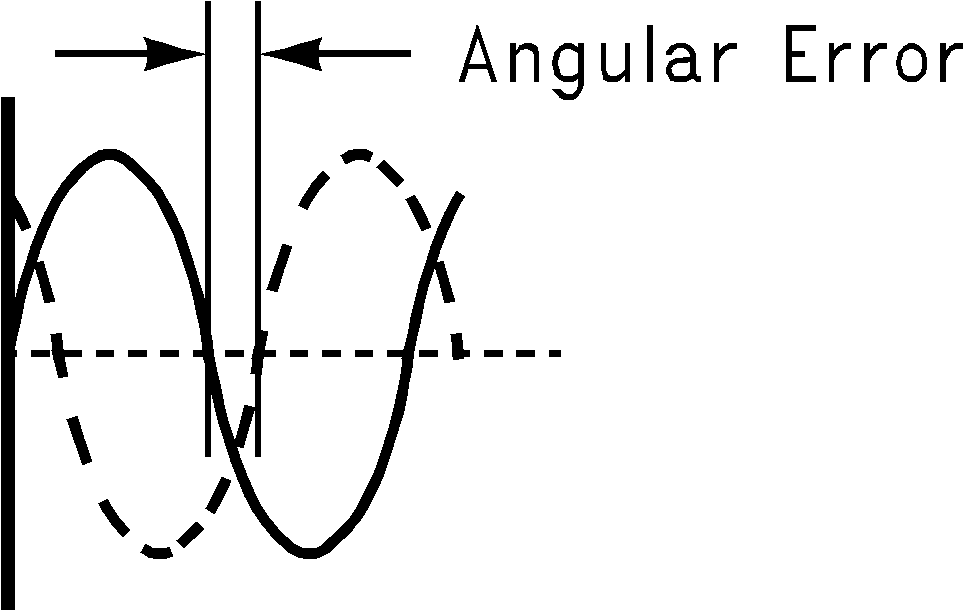
Where dev is the angular difference in degrees between the two signals having a 180° relative phase relationship to each other (see Figure 22). For single frequency inputs, angular errors result in a reduction of the effective full scale input. For complex waveforms, however, angular errors will result in distortion.
 Figure 22. Angular Errors Between The Two Input Signals Will Reduce The Output Level Or Cause Distortion
 It is recommended to drive the analog inputs with a source impedance less than 100 Ω. Matching the source impedance for the differential inputs will improve even ordered harmonic performance (particularly second harmonic).
Table 2 indicates the input to output relationship of the ADC14155.
Table 2. Input To Output Relationship
| VIN+ | VIN– | Binary Output | 2’s Complement Output | |
|---|---|---|---|---|
| VCM – VREF / 2 | VCM + VREF / 2 | 00 0000 0000 0000 | 10 0000 0000 0000 | Negative Full-Scale |
| VCM – VREF / 4 | VCM + VREF / 4 | 01 0000 0000 0000 | 11 0000 0000 0000 | |
| VCM | VCM | 10 0000 0000 0000 | 00 0000 0000 0000 | Mid-Scale |
| VCM + VREF / 4 | VCM – VREF / 4 | 11 0000 0000 0000 | 01 0000 0000 0000 | |
| VCM + VREF / 2 | VCM – VREF / 2 | 11 1111 1111 1111 | 01 1111 1111 1111 | Positive Full-Scale |