SNAS378L November 2008 – February 2019 ADC14155QML-SP
PRODUCTION DATA.
- 1 Features
- 2 Applications
- 3 Description
- 4 Revision History
- 5 Pin Configuration and Functions
-
6 Specifications
- 6.1 Absolute Maximum Ratings
- 6.2 ESD Ratings
- 6.3 Recommended Operating Conditions
- 6.4 Thermal Information
- 6.5 ADC14155 Converter Electrical Characteristics DC Parameters
- 6.6 ADC14155 Converter Electrical Characteristics (Continued) DYNAMIC Parameters
- 6.7 ADC14155 Converter Electrical Characteristics (Continued) Logic and Power Supply Electrical Characteristics
- 6.8 ADC14155 Converter Electrical Characteristics (Continued) Timing and AC Characteristics
- 6.9 Timing Diagram
- 6.10 Transfer Characteristic
- 6.11 Typical Performance Characteristics, DNL, INL
- 6.12 Typical Performance Characteristics, Dynamic Performance
- 7 Detailed Description
- 8 Application and Implementation
- 9 Power Supply Recommendations
- 10Layout
- 11Device and Documentation Support
- 12Mechanical, Packaging, and Orderable Information
Package Options
Refer to the PDF data sheet for device specific package drawings
Mechanical Data (Package|Pins)
- NBA|48
Thermal pad, mechanical data (Package|Pins)
Orderable Information
5 Pin Configuration and Functions
NBA Package
48-Pin CFP
Top View
Pin Descriptions and Equivalent Circuits
| PIN NO. | SYMBOL | EQUIVALENT CIRCUIT | DESCRIPTION |
|---|---|---|---|
| ANALOG I/O | |||
| 4 |
VIN– |
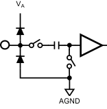 |
Differential analog input pins. The differential full-scale input signal level is two times the reference voltage with each input pin signal centered on a common mode voltage, VCM. |
| 5 | VIN+ | ||
| 42, 43 |
VRP |
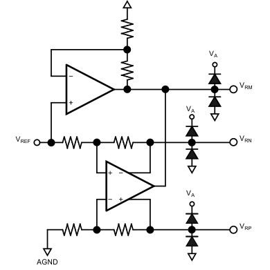 |
These pins should each be bypassed to AGND with a low ESL (equivalent series inductance) 0.1-µF capacitor placed very close to the pin to minimize stray inductance. A 0.1-µF capacitor should be placed between VRP and VRN as close to the pins as possible, and a 10-µF capacitor should be placed in parallel.
VRP and VRN should not be loaded. VRM may be loaded to 1mA for use as a temperature stable 1.5-V reference. It is recommended to use VRM to provide the common mode voltage, VCM, for the differential analog inputs, VIN+ and VIN–. |
| 46, 47 |
VRM |
||
| 44, 45 | VRN | ||
| 48 | VREF | 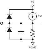 |
This pin can be used as either the 1-V internal reference voltage output (internal reference operation) or as the external reference voltage input (external reference operation).
To use the internal reference, VREF should be decoupled to AGND with a 0.1-µF, low equivalent series inductance (ESL) capacitor. In this mode, VREF defaults as the output for the internal 1.0-V reference. To use an external reference, overdrive this pin with a low noise external reference voltage. The output impedance of the internal reference at this pin is 9kΩ. Therefore, to overdrive this pin, the impedance of the external reference source should be << 9 kΩ. This pin should not be used to source or sink current. The full scale differential input voltage range is 2 * VREF. |
| DIGITAL I/O | |||
| 11 |
CLK+ |
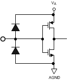 |
The clock input pins can be configured to accept either a single-ended or a differential clock input signal.
When the single-ended clock mode is selected through CLK_SEL/DF (pin 8), connect the clock input signal to the CLK+ pin and connect the CLK– pin to AGND. When the differential clock mode is selected through CLK_SEL/DF (pin 8), connect the positive and negative clock inputs to the CLK+ and CLK– pins, respectively. The analog input is sampled on the falling edge of the clock input. |
| 12 | CLK– | ||
| 8 | CLK_SEL/DF | 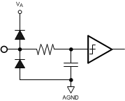 |
This is a four-state pin controlling the input clock mode and output data format.
CLK_SEL/DF = VA, CLK+ and CLK– are configured as a differential clock input. The output data format is 2's complement. CLK_SEL/DF = (2 / 3) * VA, CLK+ and CLK– are configured as a differential clock input. The output data format is offset binary. CLK_SEL/DF = (1 / 3) * VA, CLK+ is configured as a single-ended clock input and CLK– should be tied to AGND. The output data format is 2's complement. CLK_SEL/DF = AGND, CLK+ is configured as a single-ended clock input and CLK– should be tied to AGND. The output data format is offset binary. |
| 7 | PD | This is a two-state input controlling Power Down.
PD = VA, Power Down is enabled. In the Power Down state only the reference voltage circuitry remains active and power dissipation is reduced. PD = AGND, Normal operation. |
|
| 17-24,
27-32 |
D0–D13 | 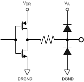 |
Digital data output pins that make up the 14-bit conversion result. D0 (pin 17) is the LSB, while D13 (pin 32) is the MSB of the output word. Output levels are CMOS compatible. |
| 33 |
OVR |
Over-Range Indicator. This output is set HIGH when the input amplitude exceeds the 14-bit conversion range (0 to 16383). | |
| 34 | DRDY | Data Ready Strobe. This pin is used to clock the output data. It has the same frequency as the sampling clock. One word of data is output in each cycle of this signal. The rising edge of this signal should be used to capture the output data. | |
| ANALOG POWER | |||
| 2, 9, 37, 40, 41 | VA | Positive analog supply pins. These pins should be connected to a quiet 3.3-V source and be bypassed to AGND with 100-pF and 0.1-µF capacitors located close to the power pins. | |
| 1, 3, 6, 10, 38, 39 | AGND | The ground return for the analog supply. | |
| DIGITAL POWER | |||
| 13 | VD | Positive digital supply pin. This pin should be connected to a quiet 3.3-V source and be bypassed to DGND with a 100-pF and 0.1-µF capacitor located close to the power pin. | |
| 14 | DGND | The ground return for the digital supply. | |
| 16, 25, 26, 36 | VDR | Positive driver supply pin for the output drivers. This pin should be connected to a quiet voltage source of 1.8 V and be bypassed to DRGND with 100-pF and 0.1-µF capacitors located close to the power pins. | |
| 15, 35 | DRGND | The ground return for the digital output driver supply. These pins should be connected to the system digital ground. See Layout Guidelines (Layout and Grounding) for more details. | |