SBAS999A June   2019  – January 2021 ADS125H01

PRODUCTION DATA  

  1. Features
  2. Applications
  3. Description
  4. Revision History
  5. Device Comparison Table
  6. Pin Configuration and Functions
  7. Specifications
    1. 7.1 Absolute Maximum Ratings
    2. 7.2 ESD Ratings
    3. 7.3 Recommended Operating Conditions
    4. 7.4 Thermal Information
    5. 7.5 Electrical Characteristics
    6. 7.6 Timing Requirements
    7. 7.7 Switching Characteristics
    8. 7.8 Timing Diagrams
    9. 7.9 Typical Characteristics
  8. Parameter Measurement Information
    1. 8.1 Noise Performance
  9. Detailed Description
    1. 9.1 Overview
    2. 9.2 Functional Block Diagram
    3. 9.3 Feature Description
      1. 9.3.1 Input Voltage Range
      2. 9.3.2 Analog Inputs (AINP, AINN)
        1. 9.3.2.1 ESD Diodes
        2. 9.3.2.2 Input Switch
      3. 9.3.3 Programmable Gain Amplifier (PGA)
        1. 9.3.3.1 PGA Operating Range
        2. 9.3.3.2 PGA Monitors
      4. 9.3.4 Reference Voltage
        1. 9.3.4.1 Reference Monitor
      5. 9.3.5 ADC Modulator
      6. 9.3.6 Digital Filter
        1. 9.3.6.1 Sinc Filter Mode
          1. 9.3.6.1.1 Sinc Filter Frequency Response
        2. 9.3.6.2 FIR Filter
        3. 9.3.6.3 50-Hz and 60-Hz Normal-Mode Rejection
    4. 9.4 Device Functional Modes
      1. 9.4.1 Conversion Control
        1. 9.4.1.1 Continuous-Conversion Mode
        2. 9.4.1.2 Pulse-Conversion Mode
        3. 9.4.1.3 Conversion Latency
        4. 9.4.1.4 Start-Conversion Delay
      2. 9.4.2 Clock Mode
      3. 9.4.3 Reset
        1. 9.4.3.1 Power-On Reset
        2. 9.4.3.2 Reset by RESETPin
        3. 9.4.3.3 Reset by Command
      4. 9.4.4 Calibration
        1. 9.4.4.1 Offset and Full-Scale Calibration
          1. 9.4.4.1.1 Offset Calibration Registers
          2. 9.4.4.1.2 Full-Scale Calibration Registers
        2. 9.4.4.2 Offset Calibration Command (OFSCAL)
        3. 9.4.4.3 Full-Scale Calibration Command (GANCAL)
        4. 9.4.4.4 Calibration Command Procedure
        5. 9.4.4.5 User Calibration Procedure
    5. 9.5 Programming
      1. 9.5.1 Serial Interface
        1. 9.5.1.1 Chip-Select Pins (CS1 and CS2)
        2. 9.5.1.2 Serial Clock (SCLK)
        3. 9.5.1.3 Data Input (DIN)
        4. 9.5.1.4 Data Output/Data Ready (DOUT/DRDY)
      2. 9.5.2 Data Ready (DRDY)
        1. 9.5.2.1 DRDY in Continuous-Conversion Mode
        2. 9.5.2.2 DRDY in Pulse-Conversion Mode
        3. 9.5.2.3 Data Ready by Software Polling
      3. 9.5.3 Conversion Data
        1. 9.5.3.1 Status Byte (STATUS0)
        2. 9.5.3.2 Conversion Data Format
      4. 9.5.4 Cyclic Redundancy Check (CRC)
      5. 9.5.5 Commands
        1. 9.5.5.1  General Command Format
        2. 9.5.5.2  NOP Command
        3. 9.5.5.3  RESET Command
        4. 9.5.5.4  START Command
        5. 9.5.5.5  STOP Command
        6. 9.5.5.6  RDATA Command
        7. 9.5.5.7  OFSCAL Command
        8. 9.5.5.8  GANCAL Command
        9. 9.5.5.9  RREG Command
        10. 9.5.5.10 WREG Command
    6. 9.6 Register Map
      1. 9.6.1  Device Identification (ID) Register (address = 00h) [reset = 4xh]
      2. 9.6.2  Main Status (STATUS0) Register (address = 01h) [reset = 01h]
      3. 9.6.3  Mode 0 (MODE0) Register (address = 02h) [reset = 24h]
      4. 9.6.4  Mode 1 (MODE1) Register (address = 03h) [reset = 01h]
      5. 9.6.5  Reserved (RESERVED) Register (address = 04h) [reset = 00h]
      6. 9.6.6  Mode 3 (MODE3) Register (address = 05h) [reset = 00h]
      7. 9.6.7  Reference Configuration (REF) Register (address = 06h) [reset = 05h]
      8. 9.6.8  Offset Calibration (OFCALx) Registers (address = 07h, 08h, 09h) [reset = 00h, 00h, 00h]
      9. 9.6.9  Full-Scale Calibration (FSCALx) Registers (address = 0Ah, 0Bh, 0Ch) [reset = 00h, 00h, 40h]
      10. 9.6.10 Reserved (RESERVED) Register (address = 0Dh) [reset = FFh]
      11. 9.6.11 Reserved (RESERVED) Register (address = 0Eh) [reset = 00h]
      12. 9.6.12 Reserved (RESERVED) Register (address = 0Fh) [reset = 00h]
      13. 9.6.13 MODE4 (MODE4) Register (address = 10h) [reset = 50h]
      14. 9.6.14 PGA Alarm (STATUS1) Register (address = 11h) [reset = xxh]
      15. 9.6.15 Status 2 (STATUS2) Register (address = 12h) [reset = 0xh]
  10. 10Application and Implementation
    1. 10.1 Application Information
      1. 10.1.1 Example to Determine the PGA Linear Operating Range
      2. 10.1.2 Input Signal Rate of Change (dV/dt)
      3. 10.1.3 Unused Inputs and Outputs
    2. 10.2 Typical Application
      1. 10.2.1 Design Requirements
      2. 10.2.2 Detailed Design Procedure
      3. 10.2.3 Application Curve
  11. 11Power Supply Recommendations
    1. 11.1 Power-Supply Decoupling
    2. 11.2 Analog Power-Supply Clamp
    3. 11.3 Power-Supply Sequencing
  12. 12Layout
    1. 12.1 Layout Guidelines
    2. 12.2 Layout Example
  13. 13Device and Documentation Support
    1. 13.1 Documentation Support
      1. 13.1.1 Related Documentation
    2. 13.2 Receiving Notification of Documentation Updates
    3. 13.3 Support Resources
    4. 13.4 Trademarks
    5. 13.5 Electrostatic Discharge Caution
    6. 13.6 Glossary
  14. 14Mechanical, Packaging, and Orderable Information

Package Options

Mechanical Data (Package|Pins)
Thermal pad, mechanical data (Package|Pins)
Orderable Information

FIR Filter

The finite impulse response (FIR) filter provides simultaneous rejection of 50-Hz and 60-Hz line cycle frequencies and related harmonics at data rates of 2.5 SPS, 5 SPS, 10 SPS, and 20 SPS. The conversion latency of the FIR filter is a single cycle; see Table 9-6 for detailed latency values. As illustrated in Figure 9-6, the FIR filter section receives data from the second-stage sinc filter. The FIR filter section decimates the data to yield the output data rate of 20 SPS. A variable averaging filter (sinc1) yields 10 SPS, 5 SPS, and 2.5 SPS.

As shown in Figure 9-15 and Figure 9-16, the frequency response has nulls that are positioned near 50 Hz and 60 Hz.
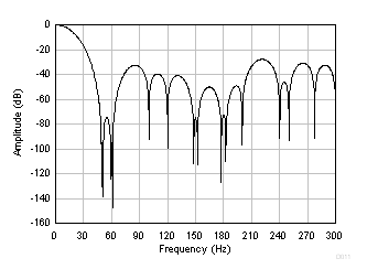
GUID-6A9C3D6D-419E-435C-88D2-C8E56FFC98AC-low.gifFigure 9-15 FIR Filter Frequency Response          (20 SPS)
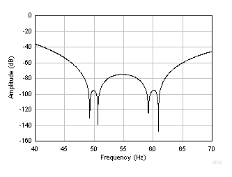
GUID-B5BDB5D7-2C30-47FB-9BE2-2652078AC772-low.gifFigure 9-16 FIR Filter Frequency Response Detail    (20 SPS)

Similar to the response of the sinc filter, the overall FIR filter frequency has a low-pass response that rolls off high frequencies. The signal bandwidth depends on the output data rate. Table 9-4 lists the –3-dB filter bandwidth of the FIR filter. The total system bandwidth is the combined response of the digital filter, the PGA antialias filter, and external filters.

Table 9-4 FIR Filter Bandwidth
DATA RATE (SPS)–3-dB BANDWIDTH (Hz)
2.51.2
52.4
104.7
2013