SBAS999A June 2019 – January 2021 ADS125H01
PRODUCTION DATA
- 1 Features
- 2 Applications
- 3 Description
- 4 Revision History
- 5 Device Comparison Table
- 6 Pin Configuration and Functions
- 7 Specifications
- 8 Parameter Measurement Information
-
9 Detailed Description
- 9.1 Overview
- 9.2 Functional Block Diagram
- 9.3 Feature Description
- 9.4 Device Functional Modes
- 9.5 Programming
- 9.6
Register Map
- 9.6.1 Device Identification (ID) Register (address = 00h) [reset = 4xh]
- 9.6.2 Main Status (STATUS0) Register (address = 01h) [reset = 01h]
- 9.6.3 Mode 0 (MODE0) Register (address = 02h) [reset = 24h]
- 9.6.4 Mode 1 (MODE1) Register (address = 03h) [reset = 01h]
- 9.6.5 Reserved (RESERVED) Register (address = 04h) [reset = 00h]
- 9.6.6 Mode 3 (MODE3) Register (address = 05h) [reset = 00h]
- 9.6.7 Reference Configuration (REF) Register (address = 06h) [reset = 05h]
- 9.6.8 Offset Calibration (OFCALx) Registers (address = 07h, 08h, 09h) [reset = 00h, 00h, 00h]
- 9.6.9 Full-Scale Calibration (FSCALx) Registers (address = 0Ah, 0Bh, 0Ch) [reset = 00h, 00h, 40h]
- 9.6.10 Reserved (RESERVED) Register (address = 0Dh) [reset = FFh]
- 9.6.11 Reserved (RESERVED) Register (address = 0Eh) [reset = 00h]
- 9.6.12 Reserved (RESERVED) Register (address = 0Fh) [reset = 00h]
- 9.6.13 MODE4 (MODE4) Register (address = 10h) [reset = 50h]
- 9.6.14 PGA Alarm (STATUS1) Register (address = 11h) [reset = xxh]
- 9.6.15 Status 2 (STATUS2) Register (address = 12h) [reset = 0xh]
- 10Application and Implementation
- 11Power Supply Recommendations
- 12Layout
- 13Device and Documentation Support
- 14Mechanical, Packaging, and Orderable Information
Package Options
Mechanical Data (Package|Pins)
- RHB|32
Thermal pad, mechanical data (Package|Pins)
- RHB|32
Orderable Information
9.3.3.1 PGA Operating Range
The absolute input voltage range of the PGA must not be exceeded in order to maintain linear operation. The maximum and minimum absolute input voltage is determined by the PGA gain setting, the maximum differential input voltage (VIN), and the minimum value of the high-voltage power supply. The absolute voltage is the combined differential and common-mode voltages. Maintain the absolute input voltage (VAINx) within the range as shown in Equation 3, otherwise incorrect conversion data can result.
where:
- Gain = PGA gain. For gain < 1, use value = 1
- V(AINx) = Absolute input voltage
- VIN = VAINP – VAINN = Maximum expected differential input voltage
Additionally, the differential input signal is limited in two conditions. The first condition is when the reference voltage exceeds AVDD – 1 V (nominally VREF > 4 V). In this case, the differential input signal is limited to: VIN = ±(AVDD – 1 V) / Gain, instead of the ideal VIN = ±VREF / Gain. The second condition applies to gains of 0.125 and 0.1875. In this case, the differential input signal range is limited to: VIN = ±20 V, regardless of the reference voltage value.
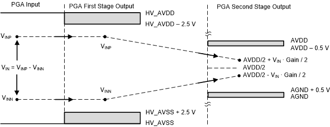
Figure 9-2 and Figure 9-3 show the relationship between the PGA input voltage and the PGA output voltage. In attenuation mode, the first PGA stage is configured as a unity-gain follower. The second PGA stage attenuates the differential input voltage and shifts the signal common-mode voltage to AVDD / 2 to drive the ADC input.
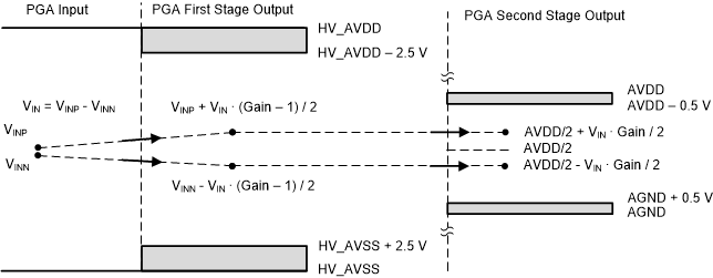
In gain mode, the first PGA stage amplifies the differential signal. The second PGA stage is configured as a unity-gain follower with level-shift. Figure 9-2 and Figure 9-3 show the corresponding output voltage of the PGA stages that must have operating voltage headroom.
 Figure 9-2 PGA
Attenuation Mode
 Figure 9-3 PGA Gain
Mode