SLUSB15J September   2012  – May 2021 BQ2947

PRODUCTION DATA  

  1. Features
  2. Applications
  3. Description
  4. Revision History
  5. Device Comparison Table
  6. Pin Configuration and Functions
  7. Specifications
    1. 7.1 Absolute Maximum Ratings
    2. 7.2 ESD Ratings
    3. 7.3 Recommended Operating Conditions
    4. 7.4 Thermal Information
    5. 7.5 Electrical Characteristics
    6. 7.6 Typical Characteristics
  8. Detailed Description
    1. 8.1 Overview
    2. 8.2 Functional Block Diagram
    3. 8.3 Feature Description
      1. 8.3.1 Pin Details
        1. 8.3.1.1 Input Sense Voltage, Vx
        2. 8.3.1.2 Output Drive, OUT
        3. 8.3.1.3 Supply Input, VDD
        4. 8.3.1.4 External Delay Capacitor, CD
    4. 8.4 Device Functional Modes
      1. 8.4.1 NORMAL Mode
      2. 8.4.2 OVERVOLTAGE Mode
      3. 8.4.3 Customer Test Mode
  9. Application and Implementation
    1. 9.1 Application Information
    2. 9.2 Typical Applications
      1. 9.2.1 Application Configuration for Active High
        1. 9.2.1.1 Design Requirements
        2. 9.2.1.2 Detailed Design Procedure
        3. 9.2.1.3 Application Curves
  10. 10Power Supply Recommendations
  11. 11Layout
    1. 11.1 Layout Guidelines
    2. 11.2 Layout Example
  12. 12Device and Documentation Support
    1. 12.1 Third-Party Products Disclaimer
    2. 12.2 Documentation Support
      1. 12.2.1 Related Documentation
    3. 12.3 Receiving Notification of Documentation Updates
    4. 12.4 Support Resources
    5. 12.5 Trademarks
    6. 12.6 Electrostatic Discharge Caution
    7. 12.7 Glossary
  13. 13Mechanical, Packaging, and Orderable Information

Package Options

Mechanical Data (Package|Pins)
Thermal pad, mechanical data (Package|Pins)
Orderable Information

Customer Test Mode

It is possible to reduce test time for checking the overvoltage function by simply shorting the external CD capacitor to VSS. In this case, the OV delay would be reduced to the t(CD_GND) value, which has a maximum of 170 ms.

Figure 8-3 shows the timing for the Customer Test Mode.
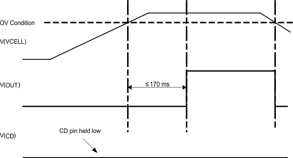
GUID-B900C3BD-7867-49EA-B624-F6745D26CF95-low.gifFigure 8-3 Timing for Customer Test Mode

Figure 8-4 shows the measurement for current consumption of the product for both VDD and Vx.
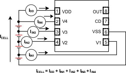
GUID-EBE7AD1B-B86C-4330-A371-708DAD14EB86-low.gifFigure 8-4 Configuration for IC Current Consumption Test