SLUSC16B November 2015 – March 2019
PRODUCTION DATA.
- 1 Features
- 2 Applications
- 3 Description
- 4 Revision History
- 5 Pin Configuration and Functions
- 6 Specifications
- 7 Detailed Description
- 8 Application and Implementation
- 9 Power Supply Recommendations
- 10Layout
- 11Device and Documentation Support
- 12Mechanical, Packaging, and Orderable Information
Package Options
Mechanical Data (Package|Pins)
- PW|16
Thermal pad, mechanical data (Package|Pins)
Orderable Information
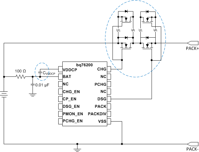
8.1.1.3 Scalable VDDCP Capacitor to Support Multiple FETs in Parallel
The bq76200 requires a minimum 470-nF capacitor to be connected between the VDDCP pin and BAT pin in order to turn on the integrated charge pump. The Electrical Characteristics Specification of this document specified the device performance based on 10 nF loading with 470-nF VDDCP capacitor. The loading capacitance varies with FET choices, number of FETs in use, and in parallel and simultaneous switching versus sequential switching of CHG and DSG FET.
The more FETs that are in parallel, the higher the loading capacitance. Similarly, simultaneously switching of the CHG and DSG FET loads down the charge pump more than sequentially switching both FETs. Eventually, the loading capacitance can exceed the supported range of a 470-nF VDDCP capacitor. A > 470-nF VDDCP capacitor can be used to support higher-loading capacitance.
 Figure 8. Scale CVDDCP to Support Multiple FETs in Parallel (Partial Schematic Shown)
 Based on test results, 470-nF VDDCP capacitor can support up to approximately 30-nF loading capacitance. Using a 470-nF/20-nF ratio (to include some design margin), a 2.1-µF VCCDP capacitor can support up to ~90-nF loading capacitance. Note that a larger VDDCP capacitor increases the charge pump start up time; a higher loading capacitance increases the FET on and off time. System designers should test across the operation range to ensure the design margin and system performance. Refer to the FET Configurations for the bq76200 High-Side N-Channel FET Driver Application Note (SLVA729) for more test results.
Also notice that any damage or disconnection of the VDDCP capacitor during operation can leave a residual voltage on the FET driver output if the inputs are enabled. This can result in putting the external FETs in a high-Rdson state and cause FET damage.