SLUSCM3K June 2016 – July 2020 BQ77904 , BQ77905
PRODUCTION DATA
- 1 Features
- 2 Applications
- 3 Description
- 4 Revision History
- 5 Device Comparison
- 6 Pin Configuration and Functions
- 7 Specifications
-
8 Detailed Description
- 8.1 Overview
- 8.2 Functional Block Diagram
- 8.3
Feature Description
- 8.3.1 Protection Summary
- 8.3.2
Fault Operation
- 8.3.2.1 Operation in OV
- 8.3.2.2 Operation in UV
- 8.3.2.3 Operation in OW
- 8.3.2.4 Operation in OCD1
- 8.3.2.5 Operation in OCD2
- 8.3.2.6 Operation in SCD
- 8.3.2.7 Overcurrent Recovery Timer
- 8.3.2.8 Load Removal Detection
- 8.3.2.9 Load Removal Detection in UV
- 8.3.2.10 Operation in OTC
- 8.3.2.11 Operation in OTD
- 8.3.2.12 Operation in UTC
- 8.3.2.13 Operation in UTD
- 8.3.3 Protection Response and Recovery Summary
- 8.3.4 Configuration CRC Check and Comparator Built-In-Self-Test
- 8.3.5 Fault Detection Method
- 8.3.6 State Comparator
- 8.3.7 DSG FET Driver Operation
- 8.3.8 CHG FET Driver Operation
- 8.3.9 External Override of CHG and DSG Drivers
- 8.3.10 Configuring 3-S, 4-S, or 5-S Mode
- 8.3.11 Stacking Implementations
- 8.3.12 Zero-Volt Battery Charging Inhibition
- 8.4 Device Functional Modes
- 9 Application and Implementation
- 10Power Supply Recommendations
- 11Layout
- 12Device and Documentation Support
- 13Mechanical, Packaging, and Orderable Information
Package Options
Mechanical Data (Package|Pins)
- PW|20
Thermal pad, mechanical data (Package|Pins)
- PW|20
Orderable Information
8.3.9 External Override of CHG and DSG Drivers
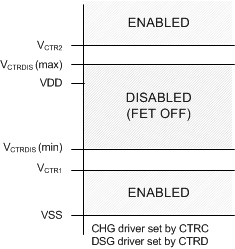
The device allows direct disabling of the CHG and DSG drivers through the CTRC and CTRD pins, respectively. The operation of the CTRC and CTRD pins is shown in Figure 8-8. To support the simple-stack solution for higher-cell count packs, these pins are designed to operate above the device’s VDD level. Simply connect a 10-MΩ resistor between a lower device CTRC and CTRD input pins to an upper device CHGU and DSG output pins (see the schematics in Section 8.3.11.
CTRC only enables or disables the CHG pin, while CTRD only enables or disables the DSG pin. When the CTRx pin is in the DISABLED region, the respective FET pin will be off, regardless of the state of the protection circuitry. When the CTRx pin is in either ENABLED region, the protection circuitry determines the state of the FET driver.
Both CTRx pins apply the fault-detection filtered method to improve the robustness of the signal detection: The counter counts up if an ENABLED signal is sampled; the counter counts down if a DISABLED signal is sampled. When the counter counts up from 0% to > 70% of its full range, which takes about 7 ms typical of a solid signal, the CTRx pins take the signal as ENABLED. If the counter counts down from 100% to < 30%, of its full range, which takes about 7 ms typical of a solid signal, the CTRx pins take the signal as DISABLED. From a 0 count counter (solid DISABLE), a solid ENABLE signal takes about tCTRDEG_ON time to deglitch. From a 100% count (solid ENABLE), a solid DISABLE signal takes about tCTRDEG_OFF time to deglitch. Although such a filter scheme provides a certain level of noise tolerance, it is highly recommended to shield the CTRx traces and keep the traces as short as possible in the PCB layout design. The CTRx deglitch time will add onto the FET response timing on the OV, UV, and OW faults in a stack configuration. The tCTRDEG_OFF time adds an additional delay to the fault detection timing and the tCTRDEG_ON time adds an additional delay to the fault recovery timing.
 Figure 8-8 External Override of CHG and DSG Drivers