SLUSCM3K June 2016 – July 2020 BQ77904 , BQ77905
PRODUCTION DATA
- 1 Features
- 2 Applications
- 3 Description
- 4 Revision History
- 5 Device Comparison
- 6 Pin Configuration and Functions
- 7 Specifications
-
8 Detailed Description
- 8.1 Overview
- 8.2 Functional Block Diagram
- 8.3
Feature Description
- 8.3.1 Protection Summary
- 8.3.2
Fault Operation
- 8.3.2.1 Operation in OV
- 8.3.2.2 Operation in UV
- 8.3.2.3 Operation in OW
- 8.3.2.4 Operation in OCD1
- 8.3.2.5 Operation in OCD2
- 8.3.2.6 Operation in SCD
- 8.3.2.7 Overcurrent Recovery Timer
- 8.3.2.8 Load Removal Detection
- 8.3.2.9 Load Removal Detection in UV
- 8.3.2.10 Operation in OTC
- 8.3.2.11 Operation in OTD
- 8.3.2.12 Operation in UTC
- 8.3.2.13 Operation in UTD
- 8.3.3 Protection Response and Recovery Summary
- 8.3.4 Configuration CRC Check and Comparator Built-In-Self-Test
- 8.3.5 Fault Detection Method
- 8.3.6 State Comparator
- 8.3.7 DSG FET Driver Operation
- 8.3.8 CHG FET Driver Operation
- 8.3.9 External Override of CHG and DSG Drivers
- 8.3.10 Configuring 3-S, 4-S, or 5-S Mode
- 8.3.11 Stacking Implementations
- 8.3.12 Zero-Volt Battery Charging Inhibition
- 8.4 Device Functional Modes
- 9 Application and Implementation
- 10Power Supply Recommendations
- 11Layout
- 12Device and Documentation Support
- 13Mechanical, Packaging, and Orderable Information
Package Options
Mechanical Data (Package|Pins)
- PW|20
Thermal pad, mechanical data (Package|Pins)
- PW|20
Orderable Information
8.3.2.8 Load Removal Detection
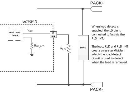
The load removal detection feature is implemented with the LD pin (see Table 8-2). When no undervoltage fault and current fault conditions are present, the LD pin is held in an open-drain state. Once any UV, OCD1, OCD2, or SCD fault occurs and load removal is selected as part of the recovery conditions, a high impedance pull-down path to VSS is enabled on the LD pin. With an external load still present, the LD pin will be externally pulled high: It is internally clamped to VLDCLAMP and should also be resistor-limited through RLD externally to avoid conducting excessive current. If the LD pin exceeds VLDT, this is interpreted as a load present condition. When the load is eventually removed, the internal high-impedance path to VSS should be sufficient to pull the LD pin below VLDT for tLD_DEG. This is interpreted as a load removed condition and is one of the recovery mechanisms selectable for undervoltage and overcurrent faults.
 Figure 8-3 Load Detection Circuit for Current Faults Recovery
| LD PIN | LOAD STATE |
|---|---|
| ≥ VLDT | Load present |
| < VLOT for tLD_DEG | Load removed |