SBOS030C August 2000 – March 2024 BUF634
PRODUCTION DATA
- 1
- 1 Features
- 2 Applications
- 3 Description
- 4 Device Comparison Table
- 5 Pin Configuration and Functions
-
6 Specifications
- 6.1 Absolute Maximum Ratings
- 6.2 ESD Ratings
- 6.3 Recommended Operating Conditions
- 6.4 Thermal Information
- 6.5 Electrical Characteristics: TO-220 and TO-263 Packages
- 6.6 Electrical Characteristics: Wide-Bandwidth Mode for SOIC Package
- 6.7 Electrical Characteristics: Low-Quiescent-Current Mode for SOIC Package
- 6.8 Typical Characteristics: TO-220 and TO-263 Packages
- 6.9 Typical Characteristics: SOIC Package
- 7 Detailed Description
- 8 Application and Implementation
- 9 Device and Documentation Support
- 10Revision History
- 11Mechanical, Packaging, and Orderable Information
Package Options
Refer to the PDF data sheet for device specific package drawings
Mechanical Data (Package|Pins)
- D|8
- KTT|5
- KC|5
Thermal pad, mechanical data (Package|Pins)
- KTT|5
Orderable Information
8.4.1 Layout Guidelines
For best operational performance of the device, use good printed circuit board (PCB) layout practices, including:
- Noise can propagate into
analog circuitry through the power pins of the circuit. Bypass capacitors
are used to reduce the coupled noise by providing low-impedance power
sources local to the analog circuitry.
- Connect low-ESR, 0.1-µF ceramic bypass capacitors between each supply pin and ground, placed as close to the device as possible. A single bypass capacitor from V+ to ground is applicable for single-supply applications.
- Separate grounding for analog and digital portions of circuitry is one of the simplest and most-effective methods of noise suppression. One or more layers on multilayer PCBs are usually devoted to ground planes. A ground plane helps distribute heat and reduces EMI noise pickup. Make sure to physically separate digital and analog grounds paying attention to the flow of the ground current. For more detailed information refer to Circuit Board Layout Techniques, SLOA089.
- To reduce parasitic coupling, run the input traces as far away from the supply or output traces as possible. If these traces cannot be kept separate, crossing the sensitive trace perpendicular is much better as opposed to in parallel with the noisy trace.
- Place the external components as close to the device as possible. As illustrated in Figure 8-9
- Keep the length of input traces as short as possible. Always remember that the input traces are the most sensitive part of the circuit.
- Clean the PCB following board assembly for best performance.
- Any precision integrated circuit can experience performance shifts due to moisture ingress into the plastic package. Following any aqueous PCB cleaning process, bake the PCB assembly to remove moisture introduced into the device packaging during the cleaning process. A low temperature, post cleaning bake at 85°C for 30 minutes is sufficient for most circumstances.
Power dissipated in the BUF634 causes the junction temperature to rise. A thermal protection circuit in the BUF634 disables the output when the junction temperature reaches approximately 175°C. When the thermal protection is activated, the output stage is disabled, allowing the device to cool. Quiescent current is approximately 6 mA during thermal shutdown. When the junction temperature cools to approximately 165°C, the output circuitry is again enabled. The die overheating can cause the protection circuit to cycle on and off with a period ranging from a fraction of a second to several minutes or more, depending on package type, signal, load and thermal environment.
The thermal protection circuit is designed to prevent damage during abnormal conditions. Any tendency to activate the thermal protection circuit during normal operation is a sign of an inadequate heat sink or excessive power dissipation for the package type.
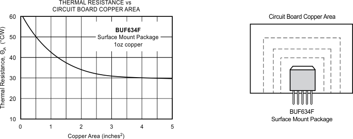
The TO-220 package provides the best thermal performance. When the TO-220 is used with a properly sized heat sink, output is not limited by thermal performance. The TO-263 also has excellent thermal characteristics; for good heat dissipation, solder the mounting tab to a circuit board copper area. Figure 8-8 shows typical thermal resistance from junction to ambient as a function of the copper area. The mounting tab of the TO-220 and TO-263 packages is electrically-connected to the V– power supply.
The DIP and SO-8 surface-mount packages are excellent for applications requiring high output current with low average power dissipation. To achieve the best possible thermal performance with the DIP or SO-8 packages, solder the device directly to a circuit board. Because much of the heat is dissipated by conduction through the package pins, sockets degrade thermal performance. Use wide circuit board traces on all the device pins, including pins that are not connected. With the DIP package, use traces on both sides of the printed circuit board if possible.
 Figure 8-8 Thermal Resistance vs Circuit Board Copper
Area