at TA = 25°C, VS
= ±15 V, RS = 50 Ω, and RL = 100 Ω (unless otherwise
noted).
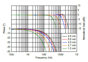
 Figure 6-19 Gain
and Phase vs Frequency and Quiescent Current
| Solid lines indicate wide-BW mode, |
| dashed lines indicate low-IQ mode |
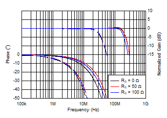
Figure 6-21 Gain
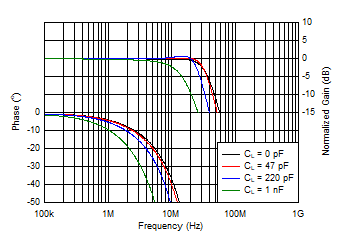
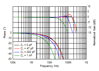
and Phase vs Frequency and Source Resistance Figure 6-23 Gain
and Phase vs Frequency and Load Capacitance
| Solid lines indicate wide-BW mode, |
| dashed lines indicate low-IQ mode |
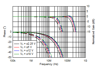
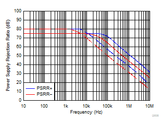
Figure 6-25 Gain
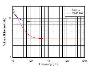
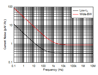
and Phase vs Frequency and Power-Supply Voltage Figure 6-27 Voltage Noise Density vs Frequency
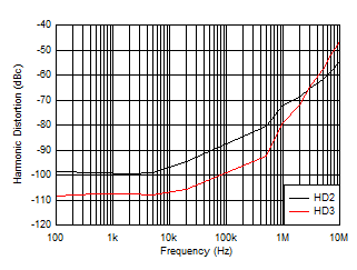
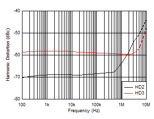
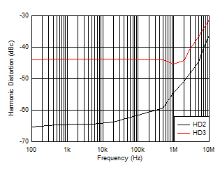
| Wide-BW mode, VIN = 10 VPP,
RL = 1 kΩ |
Figure 6-29 Harmonic Distortion vs Frequency
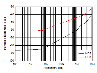
| Low-IQ mode, VIN = 10
VPP, RL = 1 kΩ |
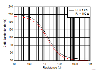
Figure 6-31 Harmonic Distortion vs Frequency Figure 6-33 Small-Signal Bandwidth vs Bandwidth Adjustment Resistance
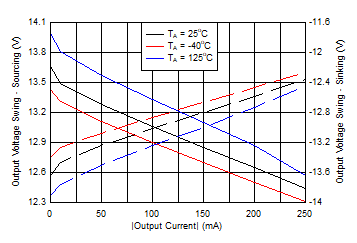
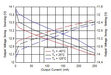
| Wide-BW mode (solid lines indicate sourcing
current, |
| dashed lines indicate sinking current) |
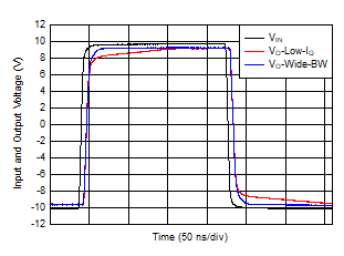
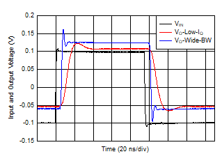
Figure 6-35 Output Voltage Swing vs Output Current Figure 6-37 Large-Signal Transient Response
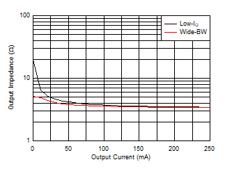
 Figure 6-39 Output Impedance vs Output Current
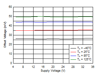
 Figure 6-41 Offset Voltage vs Supply Voltage
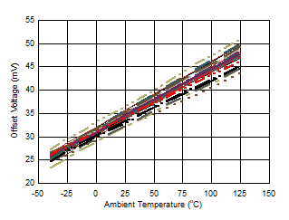
 Figure 6-43 Offset Voltage vs Temperature
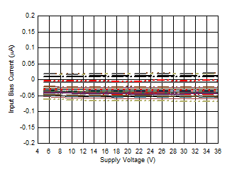
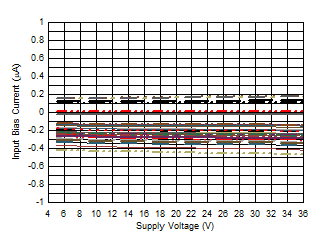
 Figure 6-45 Input
Bias Current vs Supply Voltage
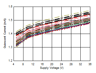
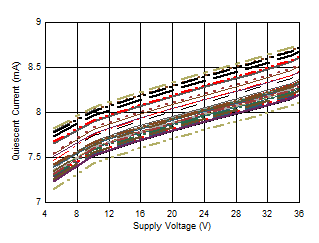
 Figure 6-47 Quiescent Current vs Supply Voltage
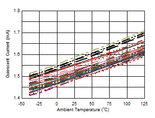
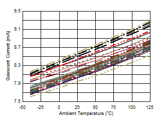
 Figure 6-49 Quiescent Current vs Temperature
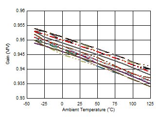
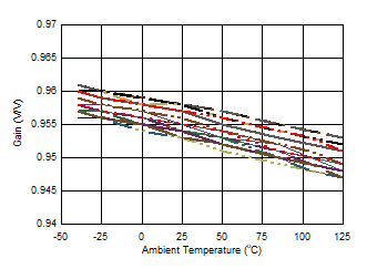
 Figure 6-51 Buffer Gain vs Temperature
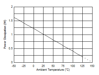
 Figure 6-53 Maximum Power Dissipation vs Temperature
| Solid lines indicate wide-BW mode, |
| dashed lines indicate low-IQ mode |
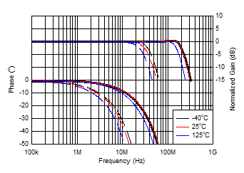
Figure 6-20 Gain
and Phase vs Frequency and Temperature
| Solid lines indicate wide-BW mode, |
| dashed lines indicate low-IQ mode |
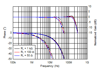
Figure 6-22 Gain
and Phase vs Frequency and Load Resistance Figure 6-24 Gain
and Phase vs Frequency and Load Capacitance
| Solid lines indicate wide-BW mode, |
| dashed lines indicate low-IQ mode |
Figure 6-26 PSRR
vs Frequency Figure 6-28 Current Noise Density vs Frequency
| Wide-BW mode, VIN = 10 VPP,
RL = 100 Ω |
Figure 6-30 Harmonic Distortion vs Frequency
| Low-IQ mode, VIN = 10
VPP, RL = 100 Ω |
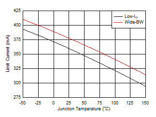
Figure 6-32 Harmonic Distortion vs Frequency Figure 6-34 Short-Circuit Current vs Temperature
| Low-IQ mode (solid lines indicate
sourcing current, |
| dashed lines indicate sinking current) |
Figure 6-36 Output Voltage Swing vs Output Current Figure 6-38 Small-Signal Transient Response
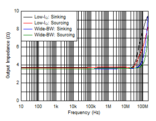
 Figure 6-40 Output Impedance vs Frequency
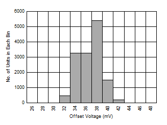
| 14000 devices, µ = 35.7 mV, σ = 2.15 mV |
Figure 6-42 Offset Voltage Distribution Histogram
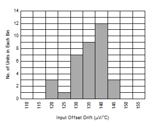
| TA = –40°C to +125°C, 35
devices, |
| µ =
134 μV/°C, σ = 7.4 μV/°C |
Figure 6-44 Offset Voltage Drift Distribution Histogram Figure 6-46 Input
Bias Current vs Supply Voltage
 Figure 6-48 Quiescent Current vs Supply Voltage
 Figure 6-50 Quiescent Current vs Temperature
 Figure 6-52 Buffer Gain vs Temperature
