SBOS948F February 2019 – May 2021 BUF634A
PRODUCTION DATA
- 1 Features
- 2 Applications
- 3 Description
- 4 Revision History
- 5 Device Comparison Table
- 6 Pin Configuration and Functions
- 7 Specifications
- 8 Detailed Description
- 9 Application and Implementation
- 10Power Supply Recommendations
- 11Layout
- 12Device and Documentation Support
- 13Mechanical, Packaging, and Orderable Information
Package Options
Refer to the PDF data sheet for device specific package drawings
Mechanical Data (Package|Pins)
- D|8
- DDA|8
- DRB|8
Thermal pad, mechanical data (Package|Pins)
Orderable Information
11.1.2 HSOIC Layout Guidelines (DDA Package With a Thermal Pad)
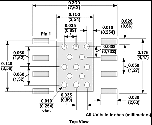
Figure 11-1 shows the DDA package top-side etch and via pattern.
 Figure 11-1 DDA Thermal Pad Integrated Circuit Package PCB Etch and Via Pattern
- Use an etch for the leads and the thermal pad.
- Place 13 vias in the thermal pad area. These vias must be 0.01 inch (0.254 mm) in diameter. Keep the vias small so that solder wicking through the vias is not a problem during reflow.
- Additional vias may be placed anywhere along the thermal plane outside of the thermal pad area, and help dissipate the heat generated by the BUF634A. These additional vias may be larger than the 0.01-inch (0.254 mm) diameter vias directly under the thermal pad because they are not in the area that requires soldering. As a result, wicking is not a problem.
- The thermal pad is internally connected with V–. Therefore, always short the thermal pad to the same potential as V– externally as well.
- Connect all vias used under the thermal pad to remove heat to the V– plane.
- When connecting these vias to the V– plane, do not use the typical web or spoke connection methodology. Web and spoke connections have a high thermal resistance that slows the heat transfer during soldering. The vias under the BUF634A thermal pad must connect to the internal thermal plane or thermal pour with a complete connection around the entire circumference of the plated-through hole.
- The top-side solder mask must leave the pins of the package and the thermal pad area with the 13 vias exposed.
- Apply solder paste to the exposed thermal pad area and all of the device pins.
- With these preparatory steps in place, the device is placed in position and run through the solder reflow operation as any standard surface-mount component.