SBOS948F February 2019 – May 2021 BUF634A
PRODUCTION DATA
- 1 Features
- 2 Applications
- 3 Description
- 4 Revision History
- 5 Device Comparison Table
- 6 Pin Configuration and Functions
- 7 Specifications
- 8 Detailed Description
- 9 Application and Implementation
- 10Power Supply Recommendations
- 11Layout
- 12Device and Documentation Support
- 13Mechanical, Packaging, and Orderable Information
Package Options
Refer to the PDF data sheet for device specific package drawings
Mechanical Data (Package|Pins)
- D|8
- DDA|8
- DRB|8
Thermal pad, mechanical data (Package|Pins)
Orderable Information
3 Description
The BUF634A device is a high-performance, high-fidelity, open-loop buffer that is capable of driving 250 mA of output current. The BUF634A is a 36-V device with an adjustable bandwidth of 35 MHz to 210 MHz, which is accomplished by varying the value of an external resistor between the V– and BW pins.
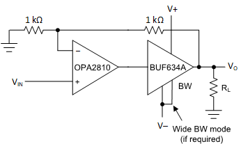
The BUF634A device can be used as a standalone open-loop driver, or used inside the feedback loop of a precision op amp to provide both high-precision and large output current drive with improved capacitive load drive.
For low-power applications, the BUF634A device operates on a 1.5-mA quiescent current with a 250-mA output, 3750-V/µs slew rate, and 35-MHz bandwidth. The device consumes 8.5-mA quiescent current in wide-bandwidth mode with a 210-MHz bandwidth. The BUF634A is fully protected by an internal current limit in its output stage and by thermal shutdown, making the device rugged and easy to use.
The BUF634A device is rated to function over the extended industrial temperature range of –40°C to +125°C. The BUF634A comes in three packages: D (SOIC), DRB (VSON), and DDA (HSOIC). The DRB (VSON) and DDA (HSOIC) packages have excellent thermal performance resulting from the thermal pad on the bottom side. The DRB package comes in a very small form factor of 3.0 mm × 3.0 mm, making the device a very suitable option for portable and size-constrained applications.
| PART NUMBER | PACKAGE | BODY SIZE (NOM) |
|---|---|---|
| BUF634A | SOIC (8) | 4.90 mm × 3.90 mm |
| VSON (8) | 3.00 mm × 3.00 mm | |
| HSOIC (8) | 4.90 mm × 3.90 mm |
 Boost the Output
Current of Any Operational Amplifier
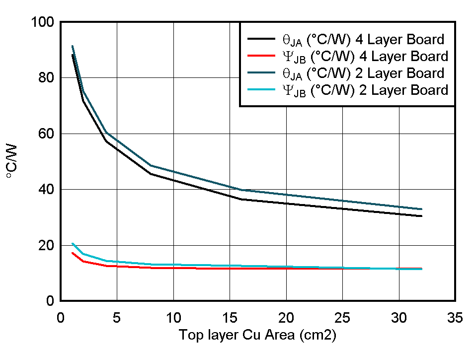
 Thermal Performance
vs Cu Area for the DDA Package