SCAS671B October 2001 – January 2022 CDCVF25081
PRODUCTION DATA
- 1 Features
- 2 Applications
- 3 Description
- 4 Revision History
- 5 Pin Configuration and Functions
- 6 Specifications
- 7 Parameter Measurement Information
- 8 Detailed Description
- 9 Application and Implementation
- 10Power Supply Recommendations
- 11Layout
- 12Device and Documentation Support
- 13Mechanical, Packaging, and Orderable Information
Package Options
Refer to the PDF data sheet for device specific package drawings
Mechanical Data (Package|Pins)
- PW|16
- D|16
Thermal pad, mechanical data (Package|Pins)
Orderable Information
6.8 Typical Characteristics
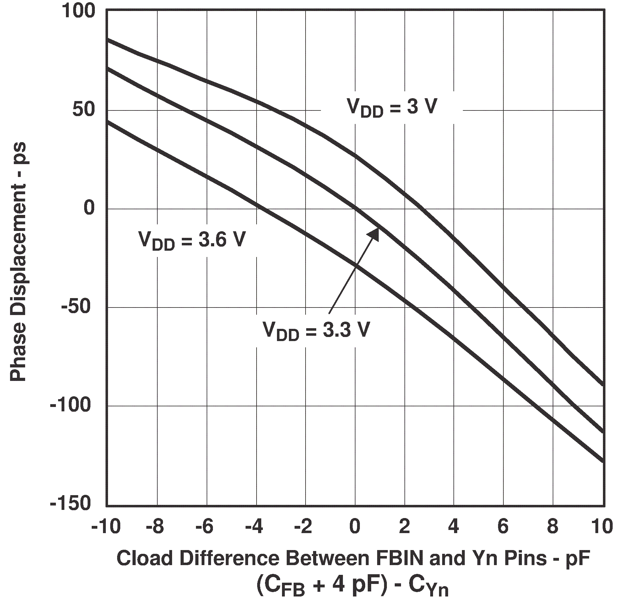
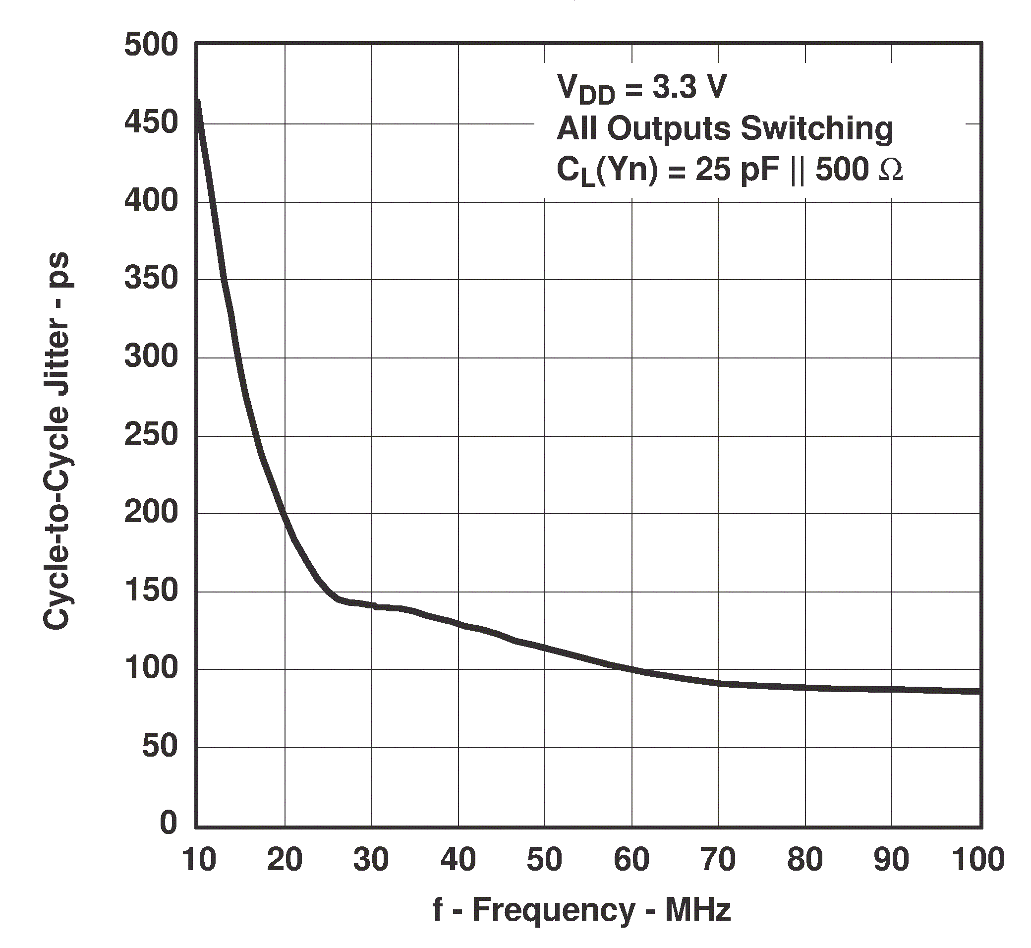
Figure 6-1 captures the variation of the CDCVF25081 current consumption with capacitive load and phase displacement. Figure 6-2 shows the variation of the cycle-to-cycle jitter across frequency.
It is important to note that Figure 6-1 and Figure 6-2 serve as a guidance to users on what to expect for the range of operating frequency supported by CDCVF25081. These graphs were plotted for a limited number of frequencies and load conditions, which may not represent the customer system.
 Figure 6-1 Phase
Displacement vs. Load