SLPS387C January 2016 – November 2023 CSD17552Q3A
PRODUCTION DATA
- 1
- 1Features
- 2Applications
- 3Description
- 4Specifications
- 5Device and Documentation Support
- 6Revision History
- 7Mechanical, Packaging, and Orderable Information
Package Options
Mechanical Data (Package|Pins)
- DNH|8
Thermal pad, mechanical data (Package|Pins)
Orderable Information
3 Description
This 30 V, 5.5 mΩ, 3.3 mm × 3.3 mm SON NexFET™ power MOSFET is designed to minimize losses in power conversion applications.
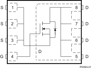
 Top View
Product Summary
| TA = 25°C | TYPICAL VALUE | UNIT | ||
|---|---|---|---|---|
| VDS | Drain-to-Source Voltage | 30 | V | |
| Qg | Gate Charge Total (4.5 V) | 9.0 | nC | |
| Qgd | Gate Charge Gate-to-Drain | 2.3 | nC | |
| RDS(on) | Drain-to-Source On Resistance | VGS = 4.5 V | 6.5 | mΩ |
| VGS = 10 V | 5.5 | mΩ | ||
| VGS(th) | Threshold Voltage | 1.5 | V | |
Ordering Information(1)
| DEVICE | QTY | MEDIA | PACKAGE | SHIP |
|---|---|---|---|---|
| CSD17552Q3A | 2500 | 13-Inch Reel | SON 3.3 mm × 3.3 mm Plastic Package |
Tape and Reel |
| CSD17552Q3AT | 250 | 7-Inch Reel |
(1) For all available packages, see the orderable addendum at the
end of the data sheet.
Absolute Maximum Ratings
| TA = 25°C unless otherwise stated | VALUE | UNIT | |
|---|---|---|---|
| VDS | Drain-to-Source Voltage | 30 | V |
| VGS | Gate-to-Source Voltage | ±20 | V |
| ID | Continuous Drain Current, TC = 25°C | 60 | A |
| Continuous Drain Current, Silicon Limited | 74 | A | |
| Continuous Drain Current, TA = 25°C(1) | 15 | A | |
| IDM | Pulsed Drain Current, TA = 25°C(2) | 84 | A |
| PD | Power Dissipation(1) | 2.6 | W |
| TJ, Tstg |
Operating Junction Temperature, Storage Temperature |
–55 to 150 | °C |
| EAS | Avalanche Energy, single pulse ID = 30 A, L = 0.1 mH, RG = 25 Ω |
45 | mJ |
(1) Typical RθJA = 48°C/W on a 1 inch2 (6.45
cm2),
2 oz. (0.071 mm thick) Cu pad on a 0.06 inch (1.52 mm) thick FR4 PCB.
2 oz. (0.071 mm thick) Cu pad on a 0.06 inch (1.52 mm) thick FR4 PCB.
(2) Pulse duration ≤300 μs, duty cycle ≤2%
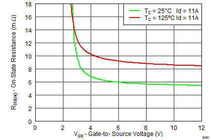
 RDS(on) vs
VGS
 |
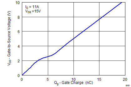
 Gate Charge
 |