SLPS458A December 2013 – August 2014 CSD95373AQ5M
PRODUCTION DATA.
- 1 Features
- 2 Applications
- 3 Description
- 4 Revision History
- 5 Pin Configuration And Functions
- 6 Specifications
- 7 Detailed Description
- 8 Application and Implementation
- 9 Layout
- 10Application Schematic
- 11Device and Documentation Support
- 12Mechanical, Packaging, and Orderable Information
Package Options
Mechanical Data (Package|Pins)
- DQP|12
Thermal pad, mechanical data (Package|Pins)
Orderable Information
8 Application and Implementation
8.1 Application Information
The Power Stage CSD95373AQ5M is a highly optimized design for synchronous buck applications using NexFET devices with a 5 V gate drive. The Control FET and Sync FET silicon are parametrically tuned to yield the lowest power loss and highest system efficiency. As a result, a rating method is used that is tailored towards a more systems centric environment. The high-performance gate driver IC integrated in the package helps minimize the parasitics and results in extremely fast switching of the power MOSFETs. System level performance curves such as Power Loss, Safe Operating Area, and normalized graphs allow engineers to predict the product performance in the actual application.
8.1.1 Power Loss Curves
MOSFET centric parameters such as RDS(ON) and Qgd are primarily needed by engineers to estimate the loss generated by the devices. To simplify the design process for engineers, TI has provided measured power loss performance curves. Figure 2 plots the power loss of the CSD95373AQ5M as a function of load current. This curve is measured by configuring and running the CSD95373AQ5M as it would be in the final application. The measured power loss is the CSD95373AQ5M device power loss, which consists of both input conversion loss and gate drive loss. Equation 1 is used to generate the power loss curve.
The power loss curve in Figure 2 is measured at the maximum recommended junction temperature of
TJ = 125°C under isothermal test conditions.
8.1.2 Safe Operating Curves (SOA)
The SOA curves in the CSD95373AQ5M data sheet give engineers guidance on the temperature boundaries within an operating system by incorporating the thermal resistance and system power loss. Figure 4 and Figure 5 outline the temperature and airflow conditions required for a given load current. The area under the curve dictates the safe operating area. All the curves are based on measurements made on a PCB design with dimensions of 4" (W) × 3.5" (L) × 0.062" (T) and 6 copper layers of 1 oz. copper thickness.
8.1.3 Normalized Curves
The normalized curves in the CSD95373AQ5M data sheet give engineers guidance on the Power Loss and SOA adjustments based on their application specific needs. These curves show how the power loss and SOA boundaries adjust for a given set of systems conditions. The primary y-axis is the normalized change in power loss and the secondary y-axis is the change is system temperature required in order to comply with the SOA curve. The change in power loss is a multiplier for the Power Loss curve and the change in temperature is subtracted from the SOA curve.
8.1.4 Calculating Power Loss And SOA
The user can estimate product loss and SOA boundaries by arithmetic means (see the Design Example). Though the Power Loss and SOA curves in this data sheet are taken for a specific set of test conditions, the following procedure outlines the steps engineers should take to predict product performance for any set of system conditions.
8.1.4.1 Design Example
Operating Conditions: Output Current (lOUT) = 30 A, Input Voltage (VIN ) = 7 V, Output Voltage (VOUT) = 1.5 V, Switching Frequency (ƒSW) = 800 kHz, Output Inductor (LOUT) = 0.2 µH.
8.1.4.2 Calculating Power Loss
- Typical Power Loss at 30 A = 4.5 W (Figure 2)
- Normalized Power Loss for switching frequency ≈ 1.07 (Figure 6)
- Normalized Power Loss for input voltage ≈ 1.07 (Figure 7)
- Normalized Power Loss for output voltage ≈ 1.06 (Figure 8)
- Normalized Power Loss for output inductor ≈ 1.02 (Figure 9)
- Final calculated Power Loss = 4.5 W × 1.07 × 1.07 × 1.06 × 1.02 ≈ 5.6 W
8.1.4.3 Calculating SOA Adjustments
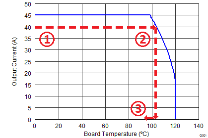 Figure 16. Power Stage CSD95373AQ5M SOA
In the previous design example, the estimated power loss of the CSD95373AQ5M would increase to 5.6 W. In addition, the maximum allowable board or ambient temperature, or both, would have to decrease by 5.7°C. Figure 16 graphically shows how the SOA curve would be adjusted accordingly.
- Start by drawing a horizontal line from the application current to the SOA curve.
- Draw a vertical line from the SOA curve intercept down to the board/ambient temperature.
- Adjust the SOA board or ambient temperature by subtracting the temperature adjustment value.
In the design example, the SOA temperature adjustment yields a reduction in allowable board/ambient temperature of 5.7°C. In the event the adjustment value is a negative number, subtracting the negative number would yield an increase in allowable board or ambient temperature.