SLPS458A December   2013  – August 2014 CSD95373AQ5M

PRODUCTION DATA.  

  1. Features
  2. Applications
  3. Description
  4. Revision History
  5. Pin Configuration And Functions
  6. Specifications
    1. 6.1 Absolute Maximum Ratings
    2. 6.2 Handling Ratings
    3. 6.3 Recommended Operating Conditions
    4. 6.4 Thermal Information
    5. 6.5 Electrical Characteristics
    6. 6.6 Typical Power Stage Device Characteristics
  7. Detailed Description
    1. 7.1 Functional Block Diagram
    2. 7.2 Feature Description
      1. 7.2.1 Powering CSD95373AQ5M And Gate Drivers
      2. 7.2.2 Undervoltage Lockout Protection (UVLO)
      3. 7.2.3 Enable
      4. 7.2.4 Power-Up Sequencing
      5. 7.2.5 PWM
      6. 7.2.6 FCCM
      7. 7.2.7 TAO/Fault (Thermal Analog Output/Protection Flag)
        1. 7.2.7.1 Overtemperature
        2. 7.2.7.2 Gate Drivers
  8. Application and Implementation
    1. 8.1 Application Information
      1. 8.1.1 Power Loss Curves
      2. 8.1.2 Safe Operating Curves (SOA)
      3. 8.1.3 Normalized Curves
      4. 8.1.4 Calculating Power Loss And SOA
        1. 8.1.4.1 Design Example
        2. 8.1.4.2 Calculating Power Loss
        3. 8.1.4.3 Calculating SOA Adjustments
  9. Layout
    1. 9.1 Layout Guidelines
      1. 9.1.1 Recommended Schematic Overview
      2. 9.1.2 Recommended PCB Design Overview
      3. 9.1.3 Electrical Performance
      4. 9.1.4 Thermal Performance
      5. 9.1.5 Sensing Performance
  10. 10Application Schematic
  11. 11Device and Documentation Support
    1. 11.1 Trademarks
    2. 11.2 Electrostatic Discharge Caution
    3. 11.3 Glossary
  12. 12Mechanical, Packaging, and Orderable Information
    1. 12.1 Mechanical Drawing
    2. 12.2 Recommended PCB Land Pattern
    3. 12.3 Recommended Stencil Opening

Package Options

Mechanical Data (Package|Pins)
Thermal pad, mechanical data (Package|Pins)
Orderable Information

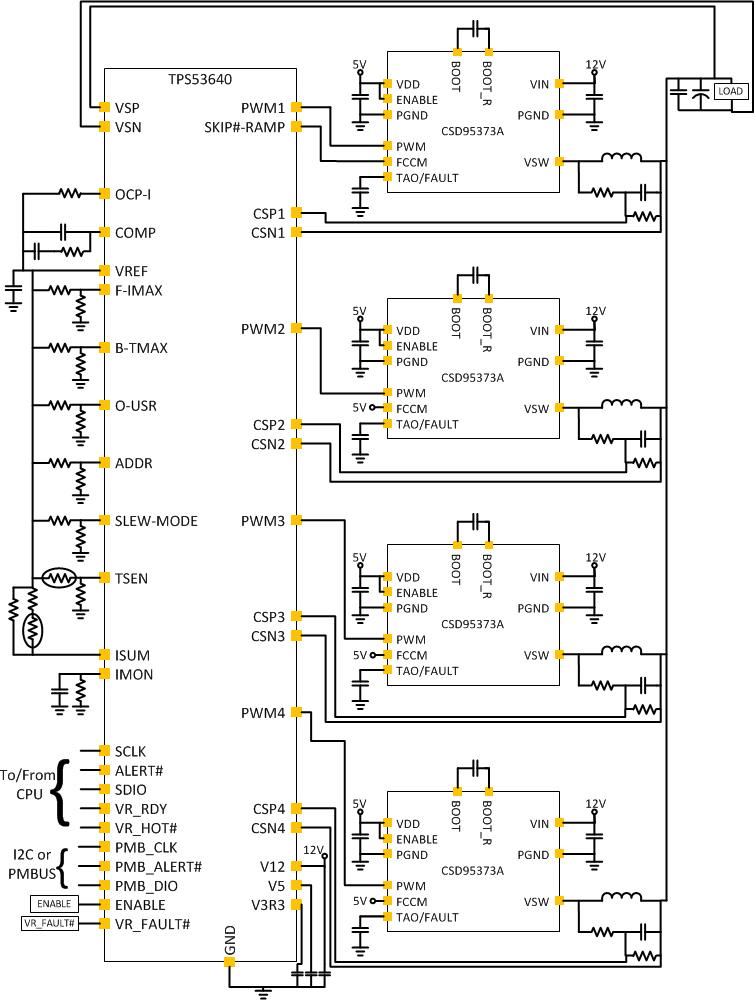
10 Application Schematic

Application.gif