SBAS246B December 2001 – November 2014 DAC8532
PRODUCTION DATA.
- 1 Features
- 2 Applications
- 3 Description
- 4 Simplified Diagram
- 5 Revision History
- 6 Pin Configuration and Functions
- 7 Specifications
- 8 Detailed Description
-
9 Application and Implementation
- 9.1 Application Information
- 9.2 Typical Application
- 10Power Supply Recommendations
- 11Layout
- 12Device and Documentation Support
- 13Mechanical, Packaging, and Orderable Information
Package Options
Refer to the PDF data sheet for device specific package drawings
Mechanical Data (Package|Pins)
- DGK|8
Thermal pad, mechanical data (Package|Pins)
Orderable Information
9 Application and Implementation
NOTE
Information in the following applications sections is not part of the TI component specification, and TI does not warrant its accuracy or completeness. TI’s customers are responsible for determining suitability of components for their purposes. Customers should validate and test their design implementation to confirm system functionality.
9.1 Application Information
9.1.1 Current Consumption
The DAC8532 typically consumes 250 µA at VDD = 5 V and 225 µA at VDD = 3 V for each active channel, including reference current consumption. Additional current consumption can occur at the digital inputs if VIH<<VDD. For most efficient power operation, CMOS logic levels are recommended at the digital input to the DAC.
In power-down mode, typical current consumption is 200 nA. A delay time of 10 to 20 ms after a power-down command is issued to the DAC is typically sufficient for the power-down current to drop below 10 µA.
9.1.2 Driving Resistive and Capacitive Loads
The DAC8532 output stage is capable of driving loads of up to 1000 pF while remaining stable. Within the offset and gain error margins, the DAC8532 can operate rail-to-rail when driving a capacitive load. Resistive loads of 2 kΩ can be driven by the DAC8532 while achieving a typical load regulation of 1%. As the load resistance drops below 2 kΩ, the load regulation error increases. When the outputs of the DAC are driven to the positive rail under resistive loading, the PMOS transistor of each Class-AB output stage can enter into the linear region. When this occurs, the added IR voltage drop deteriorates the linearity performance of the DAC. This only occurs within approximately the top 20 mV of the DAC's digital input-to-voltage output transfer characteristic. The reference voltage applied to the DAC8532 may be reduced below the supply voltage applied to VDD in order to eliminate this condition if good linearity is a requirement at full scale (under resistive loading conditions).
9.1.3 Crosstalk and AC Performance
The DAC8532 architecture uses separate resistor strings for each DAC channel in order to achieve ultra-low crosstalk performance. DC crosstalk seen at one channel during a full-scale change on the neighboring channel is typically less than 0.5LSBs. The AC crosstalk measured (for a full-scale, 1 kHz sine wave output generated at one channel, and measured at the remaining output channel) is typically under –100 dB, In addition, the DAC8532 can achieve typical AC performance of 96 dB signal-to-noise ratio (SNR) and 65 dB total harmonic distortion (THD), making the DAC8532 a solid choice for applications requiring low SNR at output frequencies at or below 4 kHz.
9.1.4 Output Voltage Stability
The DAC8532 exhibits excellent temperature stability of 5 ppm/°C typical output voltage drift over the specified temperature range of the device. This enables the output voltage of each channel to stay within a ±25 µV window for a ±1°C ambient temperature change. Good power-supply rejection ratio (PSRR) performance reduces supply noise present on VDD from appearing at the outputs to well below 10 µV-s. Combined with good DC noise performance and true 16-bit differential linearity, the DAC8532 becomes a perfect choice for closed-loop control applications.
9.1.5 Settling Time and Output Glitch Performance
Settling time to within the 16-bit accurate range of the DAC8532 is achievable within 10 µs for a full-scale code change at the input. Worst case settling times between consecutive code changes is typically less than 2 µs, enabling update rates up to 500 ksps for digital input signals changing code-to-code. The high-speed serial interface of the DAC8532 is designed in order to support these high update rates.
For full-scale output swings, the output stage of each DAC8532 channel typically exhibits less than 100 mV of overshoot and undershoot when driving a 200 pF capacitive load. Code-to-code change glitches are extremely low (~10 µV) given that the code-to-code transition does not cross an Nx4096 code boundary. Due to internal segmentation of the DAC8532, code-to-code glitches occur at each crossing of an Nx4096 code boundary. These glitches can approach 100 mVs for N = 15, but settle out within ~2 µs.
9.1.6 Microprocessor Interfacing
The following sections describe interfacing the DAC8532 with various microprocessors.
9.1.6.1 DAC8532 to 8051 Interface
Figure 36 shows a serial interface between the DAC8532 and a typical 8051-type microcontroller. The setup for the interface is as follows: TXD of the 8051 drives SCLK of the DAC8532, while RXD drives the serial data line of the device. The SYNC signal is derived from a bit-programmable pin on the port of the 8051. In this case, port line P3.3 is used. When data is to be transmitted to the DAC8532, P3.3 is taken LOW. The 8051 transmits data in 8-bit bytes; thus only eight falling clock edges occur in the transmit cycle. To load data to the DAC, P3.3 is left LOW after the first eight bits are transmitted, then a second and third write cycle is initiated to transmit the remaining data. P3.3 is taken HIGH following the completion of the third write cycle. The 8051 outputs the serial data in a format which presents the LSB first, while the DAC8532 requires its data with the MSB as the first bit received. The 8051 transmit routine must therefore take this into account, and mirror the data as needed
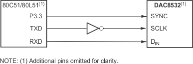 Figure 36. DAC8532 to 80C51/80L51 Interface
9.1.6.2 DAC8532 to Microwire Interface
Figure 37 shows an interface between the DAC8532 and any Microwire compatible device. Serial data is shifted out on the falling edge of the serial clock and is clocked into the DAC8532 on the rising edge of the SK signal.
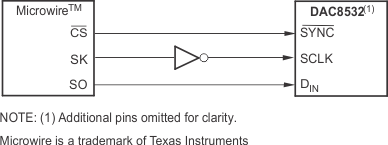 Figure 37. DAC8532 to Microwire Interface
9.1.6.3 DAC8532 to 68HC11 Interface
Figure 38 shows a serial interface between the DAC8532 and the 68HC11 microcontroller. SCK of the 68HC11 drives the SCLK of the DAC8532, while the MOSI output drives the serial data line of the DAC. The SYNC signal is derived from a port line (PC7), similar to the 8051 diagram.
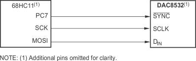 Figure 38. DAC8532 to 68HC11 Interface
The 68HC11 should be configured so that its CPOL bit is 0 and its CPHA bit is 1. This configuration causes data appearing on the MOSI output to be valid on the falling edge of SCK. When data is being transmitted to the DAC, the SYNC line is held LOW (PC7). Serial data from the 68HC11 is transmitted in 8-bit bytes with only eight falling clock edges occurring in the transmit cycle. (Data is transmitted MSB first.) In order to load data to the DAC8532, PC7 is left LOW after the first eight bits are transferred, then a second and third serial write operation is performed to the DAC. PC7 is taken HIGH at the end of this procedure.
9.1.7 DAC8532 to TMS320 DSP Interface
Figure 39 shows the connections between the DAC8532 and a TMS320 digital signal processor. By decoding the FSX signal, multiple DAC8532s can be connected to a single serial port of the DSP.
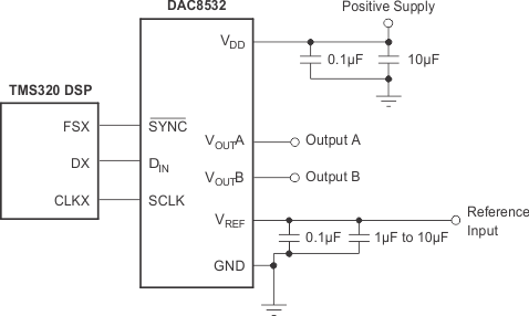 Figure 39. DAC8532 to TMS320 DSP
9.1.8 Bipolar Operation Using the DAC8532
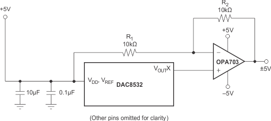 Figure 40. Bipolar Operation with the DAC8532
The DAC8532 has been designed for single-supply operation but a bipolar output range is also possible using the circuit in Figure 40. The circuit shown will give an output voltage range of ±VREF. Rail-to-rail operation at the amplifier output is achievable using an amplifier such as the OPA703, see Figure 40.
The output voltage for any input code can be calculated as follows:
where D represents the input code in decimal (0–65535).
With VREF = 5 V, R1 - R2 = 10 kΩ.
This is an output voltage range of ±5 V with 0000H corresponding to a –5 V output and FFFFH corresponding to a 5 V output. Similarly, using VREF = 2.5 V, a ±2.5 V output voltage range can be achieved.
9.2 Typical Application
9.2.1 Using REF5050 as a Power Supply for DAC8532
Due to the extremely low supply current required by the DAC8532, a possible configuration is to use the REF5050, a 5 V precision voltage reference, as the power supply and the reference for the DAC8532 . This configuration is shown in Figure 41. This is especially useful if the power supply is noisy or if 5 V is not readily available as the system supply. This configuration has the drawback of not being able to reach full scale voltage. The output buffer of the DAC requires headroom between the power supply and the reference to generate an output voltage near the reference voltage without distortion or clipping.
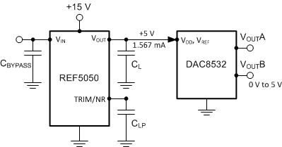 Figure 41. REF5050 as a Power Supply to the DAC8532
9.2.1.1 Design Requirements
The REF5050 requires three capacitors for operation:
- A supply bypass capacitor (CBYPASS) ranging between 1 µF and 10 µF must be connected between the REF5050 VIN and GND pins.
- A 1 µF to 50 µF output load capacitor (CL) must be connected between the REF5050 VOUT and GND pins. The ESR of CL must be less than or equal to 1.5Ω to ensure output stability and to minimize noise.
- A 1µF filter capacitor (CLP) must be connected between TRIM/NR and GND pins. CLP forms a low pass filter with a cut-off frequency between 10 Hz and 20 Hz. This filter reduces the noise injected by the reference. Note that the use of this capacitor will increase the startup time.
The REF5050 outputs a steady supply voltage for the DAC8532. If the REF5050 is used, the current supplied to the DAC8532 is 567 µA typical and 890 µA max for VDD = 5 V. When a DAC output is loaded, the REF5050 also needs to supply the current to the load. The total typical current required (with a 5 kΩ load on a given DAC output) is:
The load regulation of the REF5050 is typically 0.005 %/mA, which results in an error of 392 µV for the 1.5 mA current drawn from it. This corresponds to a 5.13 LSB error for a 0 V to 5 V output range.
9.2.1.2 Detailed Design Procedure
The REF5050 outputs a steady supply voltage for the DAC8532. The max current consumption of DAC8532 without a resistive load on the output pin is 890 μA. If the DAC outputs are loaded, the reference must also supply the current to the DAC loads. For example, the total max current required (with a 2 kΩ load on each DAC output) is:
The REF5050 output voltage change at room temperature with a 6 mA load is 100 µV. This causes a 0.002 %FSR change on the supply; this is sufficiently small to not affect the performance of the DAC.
9.2.1.3 Application Curves
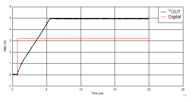
| Input Reference Voltage = 4.991250 V | ||
| Full Scale Voltage = 4.996820 V @ 0xFFFF | ||
| Zero Scale Voltage = 0.014349 V @ 0x0000 | ||
| Full Scale Settling time = 4.86 µs | ||