SBAS246B December 2001 – November 2014 DAC8532
PRODUCTION DATA.
- 1 Features
- 2 Applications
- 3 Description
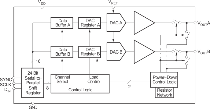
- 4 Simplified Diagram
- 5 Revision History
- 6 Pin Configuration and Functions
- 7 Specifications
- 8 Detailed Description
-
9 Application and Implementation
- 9.1 Application Information
- 9.2 Typical Application
- 10Power Supply Recommendations
- 11Layout
- 12Device and Documentation Support
- 13Mechanical, Packaging, and Orderable Information
Package Options
Refer to the PDF data sheet for device specific package drawings
Mechanical Data (Package|Pins)
- DGK|8
Thermal pad, mechanical data (Package|Pins)
Orderable Information
8 Detailed Description
8.1 Overview
The DAC8532 is a dual channel, 16-bit digital-to-analog converter (DAC) offering low power operation and a flexible serial host interface. Each on-chip precision output amplifier allows rail-to-rail output swing to be achieved over the supply range of 2.7 V to 5.5 V. The device supports a standard 3-wire serial interface capable of operating with input data clock frequencies up to 30 MHz for VDD = 5 V.
8.2 Functional Block Diagram
8.3 Feature Description
8.3.1 DAC Section
The architecture of each channel of the DAC8532 consists of a resistor string DAC followed by an output buffer amplifier. Figure 31 shows a simplified block diagram of the DAC architecture.
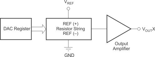 Figure 31. DAC8532 Architecture
The input coding for each device is unipolar straight binary, so the ideal output voltage is given by:
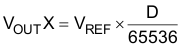
where D = decimal equivalent of the binary code that is loaded to the DAC register; it can range from 0 to 65535. VOUTX refers to channel A or B.
8.3.2 Resistor String
The resistor string section is shown in Figure 32. It is simply a divide-by-2 resistor followed by a string of resistors, each of value R. The code loaded into the DAC register determines at which node on the string the voltage is tapped off. This voltage is then applied to the output amplifier by closing one of the switches connecting the string to the amplifier.
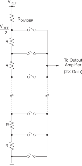 Figure 32. Resistor String
8.3.3 Output Amplifier
Each output buffer amplifier is capable of generating rail-to-rail voltages on its output which approaches an output range of 0 V to VDD (gain and offset errors must be taken into account). Each buffer is capable of driving a load of 2 kΩ in parallel with 1000 pF to GND. The source and sink capabilities of the output amplifier can be seen in the typical characteristics.
8.3.4 Serial Interface
The DAC8532 uses a 3-wire serial interface (SYNC, SCLK, and DIN), which is compatible with SPI™ and QSP™, and Microwire™ interface standards, as well as most DSPs. See the Serial Write Operation timing diagram for an example of a typical write sequence.
The write sequence begins by bringing the SYNC line LOW. Data from the DIN line is clocked into the 24-bit shift register on each falling edge of SCLK. The serial clock frequency can be as high as 30 MHz, making the DAC8532 compatible with high speed DSPs. On the 24th falling edge of the serial clock, the last data bit is clocked into the shift register and the programmed function is executed (i.e., a change in Data Buffer contents, DAC register contents, and/or a change in the power-down mode of a specified channel or channels).
At this point, the SYNC line may be kept LOW or brought HIGH. In either case, the minimum delay time from the 24th falling SCLK edge to the next falling SYNC edge must be met in order to properly begin the next cycle. To assure the lowest power consumption of the device, care should be taken that the digital input levels are as close to each rail as possible. (See the Typical Characteristics section for the Supply Current vs Logic Input Voltage transfer characteristic curve).
8.3.5 Power-On Reset
The DAC8532 contains a power-on reset circuit that controls the output voltage during power-up. On power-up, the DAC registers are filled with zeros and the output voltages are set to zero-scale; they remain there until a valid write sequence and load command is made to the respective DAC channel. This is useful in applications where it is important to know the state of the output of each DAC output while the device is in the process of powering up.
No device pin should be brought high before power is applied to the device.
8.4 Device Functional Modes
8.4.1 Input Shift Register
The input shift register of the DAC8532 is 24 bits wide (see Figure 33) and is made up of 8 control bits (DB16–DB23) and 16 data bits (DB0–DB15). The first two control bits (DB22 and DB23) are reserved and must be 0 for proper operation. LD A (DB20) and LD B (DB21) control the updating of each analog output with the specified 16-bit data value or power- down command. Bit DB19 is a Don't Care bit which does not affect the operation of the DAC8532 and can be 1 or 0. The following control bit, Buffer Select (DB18), controls the destination of the data (or power-down command) between DAC A and DAC B. The final two control bits, PD0 (DB16) and PD1 (DB17), select the power-down mode of one or both of the DAC channels. The four modes are normal mode or any one of three power-down modes. A more complete description of the operational modes of the DAC8532 can be found in the Power-Down Modes section. The remaining sixteen bits of the 24-bit input word make up the data bits. These are transferred to the specified Data Buffer or DAC Register, depending on the command issued by the control byte, on the 24th falling edge of SCLK. See Table 2 and Table 3 for more information.
| DB23 | DB12 |
| 0 | 0 | LDB | LDA | X | Buffer Select | PD1 | PD0 | D15 | D14 | D13 | D12 |
| DB11 | DB0 |
| D11 | D10 | D9 | D8 | D7 | D6 | D5 | D5 | D3 | D2 | D1 | D0 |
8.4.2 SYNC Interrupt
In a normal write sequence, the SYNC line is kept LOW for at least 24 falling edges of SCLK and the addressed DAC register is updated on the 24th falling edge. However, if SYNC is brought HIGH before the 24th falling edge, it acts as an interrupt to the write sequence; the shift register is reset and the write sequence is discarded. Neither an update of the data buffer contents, DAC register contents or a change in the operating mode occurs (see Figure 34).
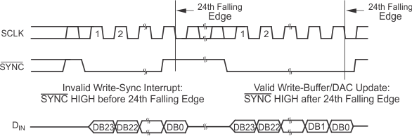 Figure 34. Interrupt and Valid SYNC Timing
8.4.3 Power-Down Modes
The DAC8532 utilizes four modes of operation. These modes are accessed by setting two bits (PD1 and PD0) in the control Load action to one or both DACs. Table 1 shows how the state of the bits correspond to the register and performing a mode of operation of each channel of the device. (Each DAC channel can be powered down simultaneously or independently of each other. Power-down occurs after proper data is written into PD0 and PD1 and a Load command occurs.) See the Operation Examples section for additional information.
Table 1. Modes of Operation for the DAC8532
| PD1 (DB17) | PD0 (DB16) | OPERATING MODE |
|---|---|---|
| 0 | 0 | Normal Operation |
| — | — | Power-down modes |
| 0 | 1 | Output typically 1 kΩ to GND |
| 1 | 0 | Output typically 100 kΩ to GND |
| 1 | 1 | High impedance |
When both bits are set to 0, the device works normally with a typical power consumption of 500 µA at 5 V. For the three power-down modes, however, the supply current falls to 200 nA at 5 V (50 nA at 3 V). Not only does the supply current fall but the output stage is also internally switched from the output of the amplifier to a resistor network of known values. This has the advantage that the output impedance of the device is known while it is in power-down mode. There are three different options for power-down: The output is connected internally to GND through a 1 kΩ resistor, a 100 kΩ resistor, or it is left open-circuited (High-Impedance). The output stage is illustrated in Figure 35.
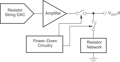 Figure 35. Output Stage During Power-Down (High Impedance)
All analog circuitry is shut down when the power-down mode is activated. Each DAC will exit power-down when PD0 and PD1 are set to 0, new data is written to the Data Buffer, and the DAC channel receives a Load command. The time to exit power-down is typically 2.5 µs for VDD = 5 V and 5 µs for VDD = 3 V (see the Typical Characteristics section.
8.5 Register Maps
Table 2. Control Matrix
| D23 | D22 | D21 | D20 | D19 | D18 | D17 | D16 | D15 | D14 | D13–D0 | DESCRIPTION |
|---|---|---|---|---|---|---|---|---|---|---|---|
| Reserved | Reserved | Load B | Load A | Don't Care | Buffer Select | PD1 | PD0 | MSB | MSB-1 | MSB-2... LSB |
|
| (Always Write 0) | 0 = A, 1 = B |
||||||||||
| 0 | 0 | 0 | 0 | X | # | 0 | 0 | Data | WR Buffer # w/Data | ||
| 0 | 0 | 0 | 0 | X | # | See Table 3 | X | WR Buffer # w/Power-down Command | |||
| 0 | 0 | 0 | 1 | X | # | 0 | 0 | Data | WR Buffer # w/Data and Load DAC A | ||
| 0 | 0 | 0 | 1 | X | 0 | See Table 3 | X | WR Buffer A w/Power-Down Command and LOAD DAC A (DAC A Powered Down) | |||
| 0 | 0 | 0 | 1 | X | 1 | See Table 3 | X | WR Buffer B w/Power-Down Command and LOAD DAC A | |||
| 0 | 0 | 1 | 0 | X | # | 0 | 0 | Data | WR Buffer # w/Data and Load DAC B | ||
| 0 | 0 | 1 | 0 | X | 0 | See Table 3 | X | WR Buffer A w/Power-Down Command and LOAD DAC B | |||
| 0 | 0 | 1 | 0 | X | 1 | See Table 3 | X | WR Buffer B w/Power-Down Command and LOAD DAC B (DAC B Powered Down) | |||
| 0 | 0 | 1 | 1 | X | # | 0 | 0 | Data | WR Buffer # w/Data and Load DACs A and B | ||
| 0 | 0 | 1 | 1 | X | 0 | See Table 3 | X | WR Buffer A w/Power-Down Command and Load DACs A and B (DAC A Powered Down) | |||
| 0 | 0 | 1 | 1 | X | 1 | See Table 3 | X | WR Buffer B w/Power-Down Command and Load DACs A and B (DAC B Powered Down) | |||
Table 3. Power-Down Commands
| D17 | D16 | OUTPUT IMPEDANCE POWER DOWN COMMANDS |
|---|---|---|
| PD1 | PD0 | |
| 0 | 1 | 1 kΩ |
| 1 | 0 | 100 kΩ |
| 1 | 1 | High Impedance |
8.5.1 Operation Examples
Example 1: Write to Data Buffer A; Through Buffer B; Load DACA Through DACB Simultaneously
- 1st — Write to DataBuffer A:
- 2nd — Write to Data Buffer B and Load DAC A and DAC B simultaneously:
| Reserved | Reserved | LDB | LDA | DC | Buffer Select | PD1 | PD0 | DB15 | — | DB1 | DB0 |
| 0 | 0 | 0 | 0 | X | 0 | 0 | 0 | D15 | — | D1 | D0 |
| Reserved | Reserved | LDB | LDA | DC | Buffer Select | PD1 | PD0 | DB15 | — | DB1 | DB0 |
| 0 | 0 | 1 | 1 | X | 1 | 0 | 0 | D15 | — | D1 | D0 |
The DACA and DACB analog outputs simultaneously settle to the specified values upon completion of the 2nd write sequence. (The Load command moves the digital data from the data buffer to the DAC register at which time the conversion takes place and the analog output is updated. Completion occurs on the 24th falling SCLK edge after SYNC LOW.)
Example 2: Load New Data to DACA and DACB Sequentially
- 1st — Write to Data Buffer A and Load DAC A: DACA output settles to specified value upon completion:
- 2nd — Write to Data Buffer B and Load DAC B: DACB output settles to specified value upon completion:
| Reserved | Reserved | LDB | LDA | DC | Buffer Select | PD1 | PD0 | DB15 | — | DB1 | DB0 |
| 0 | 0 | 0 | 1 | X | 0 | 0 | 0 | D15 | — | D1 | D0 |
| Reserved | Reserved | LDB | LDA | DC | Buffer Select | PD1 | PD0 | DB15 | — | DB1 | DB0 |
| 0 | 0 | 1 | 0 | X | 1 | 0 | 0 | D15 | — | D1 | D0 |
After completion of the 1st write cycle, the DACA analog output settles to the voltage specified; upon completion of write cycle 2, the DACB analog output settles.
Example 3: Power-Down DACA to 1 kΩ and Power-Down DACB to 100 kΩ Simultaneously
- 1st — Write power-down command to Data Buffer A:
- 2nd — Write power-down command to Data Buffer B and Load DACA and DACB simultaneously:
| Reserved | Reserved | LDB | LDA | DC | Buffer Select | PD1 | PD0 | DB15 | — | DB1 | DB0 |
| 0 | 0 | 0 | 0 | X | 0 | 0 | 1 | Don't Care | |||
| Reserved | Reserved | LDB | LDA | DC | Buffer Select | PD1 | PD0 | DB15 | — | DB1 | DB0 |
| 0 | 0 | 1 | 1 | X | 1 | 1 | 0 | Don't Care | |||
The DACA and DACB analog outputs simultaneously power-down to each respective specified mode upon completion of the 2nd write sequence.
Example 4: Power-Down DACA and DACB to High-Impedance Sequentially:
- 1st — Write power-down command to Data Buffer A and Load DAC A: DAC A output = Hi-Z:
- 2nd — Write power-down command to Data Buffer B and Load DAC B: DAC B output = Hi-Z:
| Reserved | Reserved | LDB | LDA | DC | Buffer Select | PD1 | PD0 | DB15 | — | DB1 | DB0 |
| 0 | 0 | 0 | 1 | X | 0 | 1 | 1 | Don't Care | |||
| Reserved | Reserved | LDB | LDA | DC | Buffer Select | PD1 | PD0 | DB15 | — | DB1 | DB0 |
| 0 | 0 | 1 | 0 | X | 1 | 1 | 1 | Don't Care | |||
The DACA and DACB analog outputs sequentially power-down to high-impedance upon completion of the 1st and 2nd write sequences, respectively.