SBAS246B December 2001 – November 2014 DAC8532
PRODUCTION DATA.
- 1 Features
- 2 Applications
- 3 Description
- 4 Simplified Diagram
- 5 Revision History
- 6 Pin Configuration and Functions
- 7 Specifications
- 8 Detailed Description
-
9 Application and Implementation
- 9.1 Application Information
- 9.2 Typical Application
- 10Power Supply Recommendations
- 11Layout
- 12Device and Documentation Support
- 13Mechanical, Packaging, and Orderable Information
Package Options
Refer to the PDF data sheet for device specific package drawings
Mechanical Data (Package|Pins)
- DGK|8
Thermal pad, mechanical data (Package|Pins)
Orderable Information
7 Specifications
7.1 Absolute Maximum Ratings
over operating free-air temperature range (unless otherwise noted) (1)| MIN | MAX | UNIT | ||
|---|---|---|---|---|
| VDD to GND | –0.3 | 6 | V | |
| Digital input voltage to GND | –0.3 | VDD+0.3 | ||
| VOUTA or VOUTB to GND | –0.3 | VDD+0.3 | ||
| Operating temperature range | –40 | 105 | °C | |
| TJ | 150 | |||
(1) Stresses beyond those listed under Absolute Maximum Ratings may cause permanent damage to the device. These are stress ratings only, which do not imply functional operation of the device at these or any other conditions beyond those indicated under Recommended Operating Conditions. Exposure to absolute-maximum-rated conditions for extended periods may affect device reliability.
7.2 Handling Ratings
| MIN | MAX | UNIT | |||
|---|---|---|---|---|---|
| Tstg | Storage temperature range | –65 | 150 | °C | |
| V(ESD) | Electrostatic discharge | Human body model (HBM), per ANSI/ESDA/JEDEC JS-001, all pins(1) | 1000 | V | |
| Charged device model (CDM), per JEDEC specification JESD22-C101, all pins(2) | 500 | ||||
(1) JEDEC document JEP155 states that 500-V HBM allows safe manufacturing with a standard ESD control process.
(2) JEDEC document JEP157 states that 250-V CDM allows safe manufacturing with a standard ESD control process.
7.3 Recommended Operating Conditions
all specifications –40°C to 105°C (unless otherwise noted)| MIN | NOM | MAX | UNIT | ||
|---|---|---|---|---|---|
| VDD to GND | 0 | 5.5 | V | ||
| Digital input voltage to GND | 0 | VDD | |||
| VOUTA or VOUTB to GND | 0 | VDD | |||
| Operating temperature range | –40 | 105 | °C | ||
7.4 Thermal Information
| THERMAL METRIC(1) | DAC8532 | UNIT | |
|---|---|---|---|
| DGK | |||
| 8 PINS | |||
| RθJA | Junction-to-ambient thermal resistance | 164.0 | °C/W |
| RθJC(top) | Junction-to-case (top) thermal resistance | 59.4 | |
| RθJB | Junction-to-board thermal resistance | 84.8 | |
| ψJT | Junction-to-top characterization parameter | 6.5 | |
| ψJB | Junction-to-board characterization parameter | 83.3 | |
| RθJC(bot) | Junction-to-case (bottom) thermal resistance | n/a | |
(1) For more information about traditional and new thermal metrics, see the IC Package Thermal Metrics application report, SPRA953.
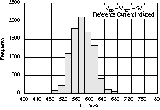
7.5 Electrical Characteristics
VDD = 2.7 V to 5.5 V, all specifications –40°C to 105°C (unless otherwise noted)| PARAMETER | TEST CONDITIONS | MIN | TYP | MAX | UNIT |
|---|---|---|---|---|---|
| STATIC PERFORMANCE(1) | |||||
| Resolution | 16 | Bits | |||
| Relative accuracy | ±0.0987 | % of FSR | |||
| Differential nonlinearity | 16-bit monotonic | ±1 | LSB | ||
| Zero code error | 5 | 25 | mV | ||
| Full-scale error | –0.15 | –1 | % of FSR | ||
| Gain error | ±1 | % of FSR | |||
| Zero code error drift | ±20 | µV/°C | |||
| Gain temperature coefficient | ±5 | ppm of FSR/°C | |||
| Channel-to-channel matching PSRR | RL = 2 kΩ, CL = 200 pF | 15 | mV | ||
| 0.75 | mV/V | ||||
| OUTPUT CHARACTERISTICS(2) | |||||
| Output voltage range | 0 | VREF | V | ||
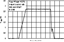
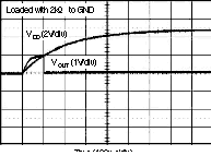
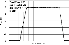
| Output voltage settling time | To ±0.003% FSR 0200H to FD00H, RL = 2 kΩ; 0 pF < CL < 200 pF, RL = 2 kΩ; CL = 500 pF |
8 | 10 | µs | |
| 12 | |||||
| Slew rate | 1 | V/µs | |||
| Capacitive load stability | RL = ∞ | 470 | pF | ||
| RL = 2 kΩ | 1000 | ||||
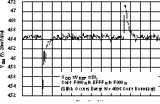
| Code change glitch impulse | 1 LSB change around major carry | 20 | nV-s | ||
| Digital feedthrough | 0.5 | nV-s | |||
| DC crosstalk | 0.25 | LSB | |||
| AC crosstalk | –100 | –96 | dB | ||
| DC output impedance | 1 | Ω | |||
| Short circuit current | VDD = 5 V | 50 | mA | ||
| VDD = 3 V | 20 | ||||
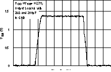
| Power-up time | Coming out of power-down mode VDD = 5 V | 2.5 | µs | ||
| Coming out of power-down mode VDD = 3 V | 5 | µs | |||
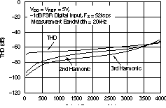
| AC PERFORMANCE | |||||
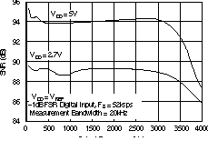
| SNR | BW = 20 kHz, VDD = 5 V, FOUT = 1 kHz, 1st 19 harmonics removed |
94 | dB | ||
| THD | 67 | ||||
| SFDR | 69 | ||||
| SINAD | 65 | ||||
| REFERENCE INPUT | |||||
| Reference current | VREF = VDD = 5 V | 67 | 90 | µA | |
| VREF = VDD = 3 V | 40 | 54 | |||
| Reference input range | 0 | VDD | V | ||
| Reference input impedance | 75 | kΩ | |||
| LOGIC INPUTS (2) | |||||
| Input current | ±1 | µA | |||
| VINL, Input LOW voltage | VDD = 5 V | 0.8 | V | ||
| VDD = 3 V | 0.6 | ||||
| VINH, Input HIGH voltage | VDD = 5 V | 2.4 | V | ||
| VDD = 3 V | 2.1 | ||||
| Pin capacitance | 3 | pF | |||
| POWER REQUIREMENTS | |||||
| VDD | 2.7 | 5.5 | V | ||
| IDD (normal mode) | DAC active and excluding load current | ||||
| VDD = 3.6 V to 5.5 V | VIH = VDD and VIL = GND | 500 | 800 | µA | |
| VDD = 2.7 V to 3.6 V | 450 | 750 | |||
| IDD (all power-down modes) | |||||
| VDD = 3.6 V to 5.5 V | VIH = VDD and VIL = GND | 0.2 | 1 | µA | |
| VDD = 2.7 V to 3.6 V | 0.05 | 1 | |||
| POWER EFFICIENCY | |||||
| IOUT/IDD | ILOAD = 2 mA, VDD = 5 V | 89% | |||
| TEMPERATURE RANGE | |||||
| Specified performance | –40 | 105 | °C | ||
(1) Linearity calculated using a reduced code range of 485 to 64714; output unloaded.
(2) Ensured by design and characterization, not production tested.
7.6 Timing Requirements (1)(2)
VDD = 2.7 V to 5.5 V, all specifications –40°C to 105°C (unless otherwise noted)| PARAMETER | TEST CONDITIONS | MIN | TYP | MAX | UNIT | |
|---|---|---|---|---|---|---|
| t1(3) | SCLK cycle time | VDD = 2.7 V to 3.6 V | 50 | ns | ||
| VDD = 3.6 V to 5.5 V | 33 | |||||
| t2 | SCLK HIGH time | VDD = 2.7 V to 3.6 V | 13 | ns | ||
| VDD = 3.6 V to 5.5 V | 13 | |||||
| t3 | SCLK LOW time | VDD = 2.7 V to 3.6 V | 22.5 | ns | ||
| VDD = 3.6 V to 5.5 V | 13 | |||||
| t4 | SYNC to SCLK rising edge setup time | VDD = 2.7 V to 3.6 V | 0 | ns | ||
| VDD = 3.6 V to 5.5 V | 0 | |||||
| t5 | Data setup time | VDD = 2.7 V to 3.6 V | 5 | ns | ||
| VDD = 3.6 V to 5.5 V | 5 | |||||
| t6 | Data hold time | VDD = 2.7 V to 3.6 V | 4.5 | ns | ||
| VDD = 3.6 V to 5.5 V | 4.5 | |||||
| t7 | 24th SCLK falling edge to SYNC rising edge | VDD = 2.7 V to 3.6 V | 0 | ns | ||
| VDD = 3.6 V to 5.5 V | 0 | |||||
| t8 | Minimum SYNC HIGH time | VDD = 2.7 V to 3.6 V | 50 | ns | ||
| VDD = 3.6 V to 5.5 V | 33 | |||||
| t9 | 24th SCLK falling edge to SYNC falling edge | VDD = 2.7 V to 5.5 V | 100 | ns | ||
(1) All input signals are specified with tR = tF = 5 ns (10% to 90% of VDD) and timed from a voltage level of (VIL + VIH)/2.
(2) See Serial Write Operation timing diagram Figure 1.
(3) Maximum SCLK frequency is 30 MHz at VDD = 3.6 V to 5.5 V and 20 MHz at VDD = 2.7 V to 3.6 V.
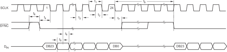 Figure 1. Serial Write Operation
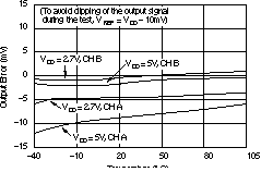
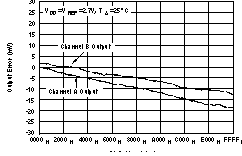
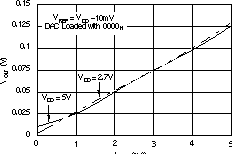
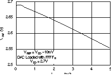
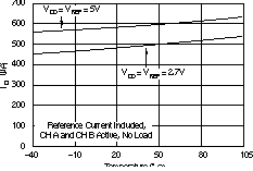
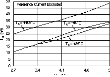
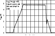
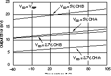
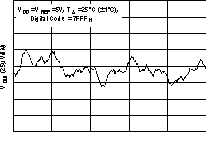
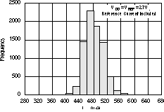
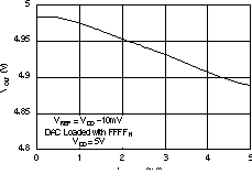
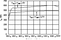
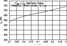
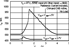
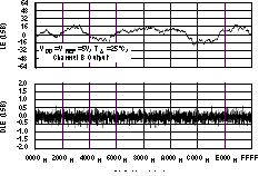
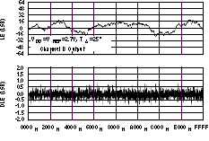
7.7 Typical Characteristics
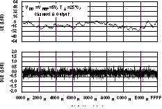
Differential Linearity Error vs Code
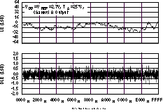
Differential Linearity Error vs Code
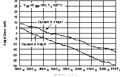
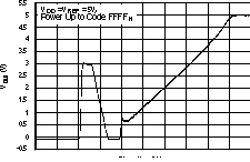
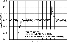
Differential Linearity Error vs Code
Differential Linearity Error vs Code