DLPS176A April 2019 – September 2019 DLP3034-Q1
PRODUCTION DATA.
- 1 Features
- 2 Applications
- 3 Description
- 4 Revision History
- 5 Pin Configuration and Functions
-
6 Specifications
- 6.1 Absolute Maximum Ratings
- 6.2 Storage Conditions
- 6.3 ESD Ratings
- 6.4 Recommended Operating Conditions
- 6.5 Thermal Information
- 6.6 Electrical Characteristics
- 6.7 Timing Requirements
- 6.8 Switching Characteristics
- 6.9 System Mounting Interface Loads
- 6.10 Physical Characteristics of the Micromirror Array
- 6.11 Micromirror Array Optical Characteristics
- 6.12 Window Characteristics
- 6.13 Chipset Component Usage Specification
- 7 Detailed Description
- 8 Application and Implementation
- 9 Power Supply Recommendations
- 10Layout
- 11Device and Documentation Support
- 12Mechanical, Packaging, and Orderable Information
Package Options
Mechanical Data (Package|Pins)
- FYJ|149
Thermal pad, mechanical data (Package|Pins)
Orderable Information
7.3.6 Temperature Sensing Diode
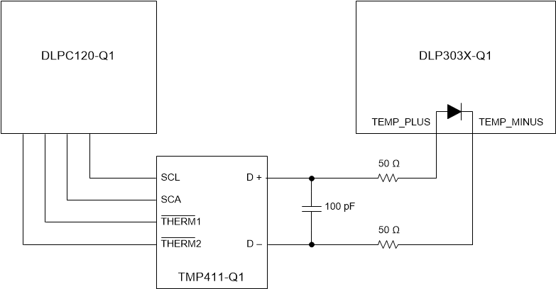
The DMD includes a temperature sensing diode designed to be used with the TMP411-Q1 temperature monitoring device. The DLPC120-Q1 monitors the DMD array temperature via the TMP411-Q1 and temperature sense diode. The DLPC120-Q1 operation of the DMD is based in part on the DMD array temperature, and therefore, this connection is essential to ensure reliable operation of the DMD.
Figure 10 shows the typical connection between the DLPC120-Q1, TMP411-Q1, and the DLP3034-Q1 DMD. The signals to the temperature sense diode are sensitive to system noise, therefore, care should be taken in the routing and implementation of this circuit. See the TMP411-Q1 Data Sheet for detailed PCB layout recommendations.
 Figure 10. Temperature Sense Diode Typical Circuit Configuration
 The DLPC120-Q1 automatically controls the DMD parking based on the temperature measured from the temperature sense diode; however, it is recommended that the host controller manage the parking via the proper methods described in the DLPC120-Q1 Programmer's Guide.