DLPS082 February   2017 DLPA100

PRODUCTION DATA.  

  1. Features
  2. Applications
  3. Description
    1. 3.1 Typical Application Diagram
  4. Revision History
  5. Pin Configuration and Functions
    1.     Pin Functions
  6. Specifications
    1. 6.1 Absolute Maximum Ratings
    2. 6.2 Storage Conditions
    3. 6.3 ESD Ratings
    4. 6.4 Recommended Operating Conditions
    5. 6.5 Thermal Information
    6. 6.6 Electrical Characteristics
  7. Detailed Description
    1. 7.1 Overview
    2. 7.2 Functional Block Diagram
    3. 7.3 Feature Description
      1. 7.3.1  Power Up Sequencing
      2. 7.3.2  Power Down Sequencing
      3. 7.3.3  Shutdown
        1. 7.3.3.1 Thermal
      4. 7.3.4  System Reset
      5. 7.3.5  Interrupt Logic
      6. 7.3.6  Serial Communications Port
      7. 7.3.7  Switching Regulators
        1. 7.3.7.1 Output Voltage - VOUT
        2. 7.3.7.2 Adjustable Linear Regulator - VLIN1
        3. 7.3.7.3 Adjustable Linear Regulator Control - VLIN2
      8. 7.3.8  Fan Controllers
      9. 7.3.9  Color Wheel Motor Driver
        1. 7.3.9.1 Color Wheel Motor Driver Power Dissipation
      10. 7.3.10 Color Wheel Switching Regulator Supply
    4. 7.4 Device Functional Modes
  8. Application and Implementation
    1. 8.1 Application Information
    2. 8.2 Typical Application
      1. 8.2.1 Design Requirements
      2. 8.2.2 Detailed Design Procedure
      3. 8.2.3 Application Curves
  9. Power Supply Recommendations
  10. 10Layout
    1. 10.1 Layout Guidelines
    2. 10.2 Grounding Guidelines
      1. 10.2.1 Completely Isolated Ground Regions
      2. 10.2.2 Single Isolated Ground Region
      3. 10.2.3 Non-isolated Common Ground Region
    3. 10.3 Thermal Guidelines
    4. 10.4 Motor Control Guidelines
    5. 10.5 Layout Example
  11. 11Device and Documentation Support
    1. 11.1 Device Markings
    2. 11.2 Documentation Support
      1. 11.2.1 Related Documentation
    3. 11.3 Community Resources
    4. 11.4 Trademarks
    5. 11.5 Electrostatic Discharge Caution
    6. 11.6 Glossary
  12. 12Mechanical, Packaging, and Orderable Information
    1. 12.1 Package Option Addendum
      1. 12.1.1 Packaging Information

Package Options

Mechanical Data (Package|Pins)
  • DLP|48
Thermal pad, mechanical data (Package|Pins)

Completely Isolated Ground Regions

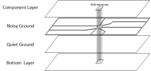
In this case, the PWB has an isolated ground layer around the DLPA100 circuit which serves as a “noisy” ground for the motor driver, switchers, and linear regulators. This plane can be subdivided into isolated sections around each switcher, linear regulator and motor block to minimize the possibility of noise crosstalk between the regulator circuits. See Figure 6. Each isolated section should be connected in a “star” configuration at the DLPA100 thermal pad position. An additional “quiet” solid ground plane should be provided on a separate layer for reference to the sensitive blocks of the DLPA100 device and other sensitive external circuitry. The sensitive pins on the DLPA100 device are pins 1, 2, 3, 4, 5, 6, 8, and 48. The quiet ground plane should connect to the DLPA100 device with the array of thermal vias.
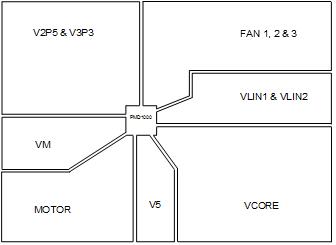
DLPA100 DLPA100_ground_layer.jpgFigure 6. Noisy Ground Layer
DLPA100 DLPA100_pwb_planes.jpgFigure 7. PWB Planes