DLPS082 February 2017 DLPA100
PRODUCTION DATA.
- 1 Features
- 2 Applications
- 3 Description
- 4 Revision History
- 5 Pin Configuration and Functions
- 6 Specifications
-
7 Detailed Description
- 7.1 Overview
- 7.2 Functional Block Diagram
- 7.3 Feature Description
- 7.4 Device Functional Modes
- 8 Application and Implementation
- 9 Power Supply Recommendations
- 10Layout
- 11Device and Documentation Support
- 12Mechanical, Packaging, and Orderable Information
Package Options
Mechanical Data (Package|Pins)
- DLP|48
Thermal pad, mechanical data (Package|Pins)
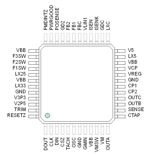
5 Pin Configuration and Functions
( PT package)
(48 pin QFP)
Top View

Pin Functions
| PIN | I/O | DESCRIPTION | |
|---|---|---|---|
| NAME | NO. | ||
| DOUT | 1 | Output | Data Out for Serial Port |
| CLK | 2 | Input | Clock for Serial Port |
| DIN | 3 | Input | Data In for Serial Port |
| CSZ | 4 | Input | Chip Select for Serial Port |
| TACH | 5 | Output | Motor Speed Indication |
| OSC | 6 | Input | Master Osc for Digital Timing – 2 MHz typical |
| GND | 7 | Ground | Ground |
| GMIN | 8 | Input | Motor Gm Input |
| VBB | 9 | Power | VBB Load Supply |
| VMSW | 10 | Output | Motor Supply Switching Node |
| VM | 11 | Input | Motor Supply INPUT/FB |
| OUTA | 12 | Output | Motor Phase A |
| CTAP | 13 | Input/Output | Motor Centertap |
| SENSE | 14 | Input | Motor Current Sensing |
| OUTB | 15 | Output | Motor Phase B |
| OUTC | 16 | Output | Motor Phase C |
| CP2 | 17 | Power | Charge Pump |
| CP1 | 18 | Power | Charge Pump |
| GND | 19 | Ground | Ground |
| VREG | 20 | Power | Internal Bias Regulator Terminal |
| VCP | 21 | Power | Charge Pump Reservoir Capacitor Terminal |
| VBB | 22 | Power | VBB Load Supply |
| LX5 | 23 | Output | 5V Regulator Switching Node |
| V5 | 24 | Power Input | 5V Feedback and Logic Supply Input |
| LXC | 25 | Power Output | Adjustable Core Regulator Switching Node |
| GDC | 26 | Power Output | Gate Drive for Core Regulator |
| ISENK | 27 | Input | Kelvin Sense for Core Regulator |
| ISEN | 28 | Input | Current Sense for Core Regulator |
| VLIN1 | 29 | Power Output | VLIN1 Linear Regulator Output |
| FBC | 30 | Power Input | Adjustable Core Switching Regulator Feedback Node |
| FB1 | 31 | Power Input | VLIN1 Adjustable Feedback Node |
| FB2 | 32 | Power Input | VLIN2 Adjustable Feedback Node |
| GD2 | 33 | Power Output | VLIN2 Linear Gate Drive Output |
| POSENSE | 34 | Output | Power On Reset Output |
| PWRGOOD | 35 | Output | Power Good Output |
| PMDINTZ | 36 | Output | Interrupt Flag |
| VBB | 37 | Power | Motor Supply Terminal |
| F3SW | 38 | Output | Fan 3 Switching Node Output |
| F2SW | 39 | Output | Fan 2 Switching Node Output |
| F1SW | 40 | Output | Fan 1 Switching Node Output |
| LX25 | 41 | Power Output | 2.5V Regulator Switching Node |
| VBB | 42 | Power | VBB Load Supply |
| LX33 | 43 | Power Output | 3.3V Regulator Switching Node |
| GND | 44 | Ground | Ground |
| V3P3 | 45 | Power Input | 3.3V Feedback |
| V2P5 | 46 | Power Input | 2.5V Feedback |
| TRIM | 47 | Power | Trim Pin (must be tied to VREG) |
| RESETZ | 48 | Input | Forced Reset |