SBOS094B January 1998 – December 2014 DRV134 , DRV135
PRODUCTION DATA.
- 1 Features
- 2 Applications
- 3 Description
- 4 Simplified Schematic
- 5 Revision History
- 6 Pin Configuration and Functions
- 7 Specifications
- 8 Detailed Description
- 9 Application and Implementation
- 10Power Supply Recommendations
- 11Layout
- 12Device and Documentation Support
- 13Mechanical, Packaging, and Orderable Information
Package Options
Mechanical Data (Package|Pins)
Thermal pad, mechanical data (Package|Pins)
- DW|16
Orderable Information
6 Pin Configuration and Functions
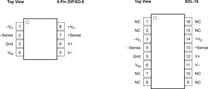
NC - No internal connection
Pin Functions
| PIN | I/O | DESCRIPTION | ||
|---|---|---|---|---|
| NAME | DIP-8 and SO-8 | SOL-16 | ||
| Gnd | 3 | 5 | – | Ground |
| +Sense | 7 | 13 | I | Sensing, non-inverting input |
| –Sense | 2 | 4 | I | Sensing, inverting input |
| V+ | 6 | 12 | – | Positive supply |
| V– | 5 | 11 | – | Negative supply |
| VIN | 4 | 6 | I | Input |
| –Vo | 1 | 3 | O | Inverted, balanced differential output |
| +Vo | 8 | 14 | O | Balanced differential output |
| NC | – | 1,2,7,8,9,10,15,16 | – | These pins should be left unconnected |