SLOS861C March 2015 – January 2023 DRV2700
PRODUCTION DATA
- 1 Features
- 2 Applications
- 3 Description
- 4 Revision History
- 5 Pin Configuration and Functions
- 6 Specifications
- 7 Detailed Description
-
8 Application and Implementation
- 8.1 Application Information
- 8.2
Typical Applications
- 8.2.1
AC-Coupled DAC Input Application
- 8.2.1.1 Design Requirements
- 8.2.1.2
Detailed Design Procedure
- 8.2.1.2.1 Piezo Load Selection
- 8.2.1.2.2 Programming The Boost Voltage
- 8.2.1.2.3 Inductor and Transformer Selection
- 8.2.1.2.4 Programing the Boost and Flyback Current-Limit
- 8.2.1.2.5 Boost Capacitor Selection
- 8.2.1.2.6 Pulldown FET and Resistors
- 8.2.1.2.7 Low-Voltage Operation
- 8.2.1.2.8 Current Consumption Calculation
- 8.2.1.2.9 Input Filter Considerations
- 8.2.1.2.10 Output Limiting Factors
- 8.2.1.2.11 Startup and Shutdown Sequencing
- 8.2.1.3 Application Curves
- 8.2.2 Filtered AC Coupled Single-Ended PWM Input Application
- 8.2.3 DC-Coupled DAC Input Application
- 8.2.4 DC-Coupled Reference Input Application
- 8.2.5 Flyback Circuit
- 8.2.1
AC-Coupled DAC Input Application
- 8.3 System Example
- 9 Power Supply Recommendations
- 10Layout
- 11Device and Documentation Support
- 12Mechanical, Packaging, and Orderable Information
Package Options
Refer to the PDF data sheet for device specific package drawings
Mechanical Data (Package|Pins)
- RGP|20
Thermal pad, mechanical data (Package|Pins)
- RGP|20
Orderable Information
8.2.1.2.10 Output Limiting Factors
Because of the small size of the DRV2700 device, limiting factors must be considered. In each of the applications, four factors can affect the output. These factors include the following:
- Bandwidth of the amplifier
- Limited current
- Slew rate
- Thermal shutdown
Although some of these factors can appear at the same time, each of these factors are shown in the following figures to help the designer differentiate between each factor.
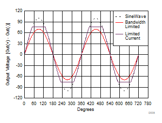
 Figure 8-4 Bandwidth and Limited Current
The internal amplifier has an inherent bandwidth limitation on the order of 5 to 20 kHz depending on the gain settings. Although, this bandwidth limitation occurs primarily with a no-load condition or under a very small voltage swing, the output is essentially unable to drive to the expected output voltage because of a drop in the gain at that bandwidth. The internal boost converter can only support a limited amount of current. If for instance, the load was somewhat resistive as opposed to only capacitive, a situation could occur where the load requires additional current to pull the voltage up, however the boost converter cannot support it. This situation appears to be an out-of-regulation output voltage.
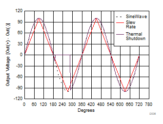
 Figure 8-5 Slew Rate and Thermal Shutdown
As the output frequency increases, the slew rate increases. Because the boost converter can only support a certain amount of current based on the load capacitance, the sine wave begins to turn into more of a triangle wave.
Lastly, the device has a thermal shutdown feature for protection from damaging when the device begins to heat up because of power dissipation. When a load is primarily capacitance, the current leads the voltage (leading power factor). With a leading or lagging power factor, the maximum power does not occur at the maximum voltage or current. However the maximum power does occur at the phase crossing of these. This occurrence looks similar to the waveform in Figure 8-5, such that the output goes to 0 V and then start back up after it has cooled down below the internal threshold. Figure 8-2 shows a general guideline to staying below the maximum voltage and frequency based on the capacitance of the load.