SLOS861C March 2015 – January 2023 DRV2700
PRODUCTION DATA
- 1 Features
- 2 Applications
- 3 Description
- 4 Revision History
- 5 Pin Configuration and Functions
- 6 Specifications
- 7 Detailed Description
-
8 Application and Implementation
- 8.1 Application Information
- 8.2
Typical Applications
- 8.2.1
AC-Coupled DAC Input Application
- 8.2.1.1 Design Requirements
- 8.2.1.2
Detailed Design Procedure
- 8.2.1.2.1 Piezo Load Selection
- 8.2.1.2.2 Programming The Boost Voltage
- 8.2.1.2.3 Inductor and Transformer Selection
- 8.2.1.2.4 Programing the Boost and Flyback Current-Limit
- 8.2.1.2.5 Boost Capacitor Selection
- 8.2.1.2.6 Pulldown FET and Resistors
- 8.2.1.2.7 Low-Voltage Operation
- 8.2.1.2.8 Current Consumption Calculation
- 8.2.1.2.9 Input Filter Considerations
- 8.2.1.2.10 Output Limiting Factors
- 8.2.1.2.11 Startup and Shutdown Sequencing
- 8.2.1.3 Application Curves
- 8.2.2 Filtered AC Coupled Single-Ended PWM Input Application
- 8.2.3 DC-Coupled DAC Input Application
- 8.2.4 DC-Coupled Reference Input Application
- 8.2.5 Flyback Circuit
- 8.2.1
AC-Coupled DAC Input Application
- 8.3 System Example
- 9 Power Supply Recommendations
- 10Layout
- 11Device and Documentation Support
- 12Mechanical, Packaging, and Orderable Information
Package Options
Refer to the PDF data sheet for device specific package drawings
Mechanical Data (Package|Pins)
- RGP|20
Thermal pad, mechanical data (Package|Pins)
- RGP|20
Orderable Information
8.2.1.2.2 Programming The Boost Voltage
The boost or flyback output voltage is programmed by an external network as shown in Figure 8-3.
 Figure 8-3 External Network
Depending on which configuration or mode is used in the system, use Equation 1 to calculate the output voltage.
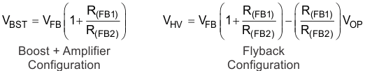
where
- VFB = 1.30 V
- VOP = VOL of the operational amplifier (op amp). Typically this can be approximated to 0 V.
The BST pin should be programmed to a value 5-V greater than the largest peak voltage in the system expected to allow adequate amplifier headroom. Because the programming range for the boost voltage extends to 105 V, the leakage current through the resistor divider becomes significant. TI recommends that the sum of the resistance of R(FB1) and R(FB2) be greater than 500 kΩ.
The flyback mode configuration may require filtering capacitors to go along with the feedback network to increase the performance at low and high frequencies. Because the charge storage is inversely proportional to the capacitance, use Equation 2 to calculate the values of the capacitors. In general, select a value of 22 pF for C(FB1).
For this design example, because the value of VPP must be negative, the boost + amplifier configuration must be used. Additionally, because the value of VBST must be 5 V more than VP, VBST is set to 65 V. Using Equation 1, the feedback resistors can be found such that RFB1 = 49 × RFB2. Because the total resistance must be greater than 500 kΩ, RFB1= 735 kΩ and RFB2= 15 kΩ.

When resistor values greater than 1 MΩ are used, PCB contamination causes boost voltage inaccuracy. Use caution when soldering large resistences, and clean the area when finished for best results.