SLVSD29 October 2015 DRV8704
PRODUCTION DATA.
- 1 Features
- 2 Applications
- 3 Description
- 4 Revision History
- 5 Pin Configuration and Functions
- 6 Specifications
-
7 Detailed Description
- 7.1 Overview
- 7.2 Functional Block Diagram
- 7.3 Feature Description
- 7.4 Device Functional Modes
- 7.5
Register Maps
- 7.5.1
Control Registers
- 7.5.1.1 CTRL Register (Address = 0x00h)
- 7.5.1.2 TORQUE Register (Address = 0x01h)
- 7.5.1.3 OFF Register (Address = 0x02h)
- 7.5.1.4 BLANK Register (Address = 0x03h)
- 7.5.1.5 DECAY Register (Address = 0x04h)
- 7.5.1.6 Reserved Register Address = 0x05h
- 7.5.1.7 DRIVE Register Address = 0x06h
- 7.5.1.8 STATUS Register (Address = 0x07h)
- 7.5.1
Control Registers
- 8 Application and Implementation
- 9 Power Supply Recommendations
- 10Layout
- 11Device and Documentation Support
- 12Mechanical, Packaging, and Orderable Information
Package Options
Mechanical Data (Package|Pins)
- DCP|38
Thermal pad, mechanical data (Package|Pins)
- DCP|38
Orderable Information
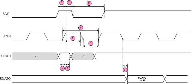
6.6 SPI Timing Requirements
over operating free-air temperature range (unless otherwise noted)| NO. | MIN | MAX | UNIT | ||
|---|---|---|---|---|---|
| 1 | tCYC | Clock cycle time | 250 | ns | |
| 2 | tCLKH | Clock high time | 25 | ns | |
| 3 | tCLCL | Clock low time | 25 | ns | |
| 4 | tSU(SDATI) | Setup time, SDATI to SCLK | 5 | ns | |
| 5 | tH(SDATI) | Hold time, SDATI to SCLK | 1 | ns | |
| 6 | tSU(SCS) | Setup time, SCS to SCLK | 5 | ns | |
| 7 | tH(SCS) | Hold time, SCS to SCLK | 1 | ns | |
| 8 | tL(SCS) | Inactive time, SCS (between writes) | 100 | ns | |
| 9 | tD(SDATO) | Delay time, SCLK to SDATO (during read) | 10 | ns | |
| tSLEEP | Wake time (SLEEPn inactive to high-side gate drive enabled) | 1 | ms | ||
| tRESET | Delay from power-up or RESETn high until serial interface functional | 10 | μs | ||
 Figure 1. Timing Diagram