SNLS456D March 2016 – October 2019 DS250DF410
PRODUCTION DATA.
- 1 Features
- 2 Applications
- 3 Description
- 4 Revision History
- 5 Description (continued)
- 6 Pin Configuration and Functions
-
7 Specifications
- 7.1 Absolute Maximum Ratings
- 7.2 ESD Ratings
- 7.3 Recommended Operating Conditions
- 7.4 Thermal Information
- 7.5 Electrical Characteristics
- 7.6 Timing Requirements, Retimer Jitter Specifications
- 7.7 Timing Requirements, Retimer Specifications
- 7.8 Timing Requirements, Recommended Calibration Clock Specifications
- 7.9 Recommended SMBus Switching Characteristics (Slave Mode)
- 7.10 Recommended SMBus Switching Characteristics (Master Mode)
- 7.11 Recommended JTAG Switching Characteristics
- 7.12 Typical Characteristics
-
8 Detailed Description
- 8.1 Overview
- 8.2 Functional Block Diagram
- 8.3
Feature Description
- 8.3.1 Device Data Path Operation
- 8.3.2 Signal Detect
- 8.3.3 Continuous Time Linear Equalizer (CTLE)
- 8.3.4 Variable Gain Amplifier (VGA)
- 8.3.5 Cross-Point Switch
- 8.3.6 Decision Feedback Equalizer (DFE)
- 8.3.7 Clock and Data Recovery (CDR)
- 8.3.8 Calibration Clock
- 8.3.9 Differential Driver with FIR Filter
- 8.3.10 Debug Features
- 8.3.11 Interrupt Signals
- 8.3.12 JTAG Boundary Scan
- 8.4 Device Functional Modes
- 8.5 Programming
- 8.6 Register Maps
- 9 Application and Implementation
- 10Power Supply Recommendations
- 11Layout
- 12Device and Documentation Support
- 13Mechanical, Packaging, and Orderable Information
Package Options
Mechanical Data (Package|Pins)
- ABM|101
Thermal pad, mechanical data (Package|Pins)
Orderable Information
9.2.3 Backplane and Mid-plane Applications
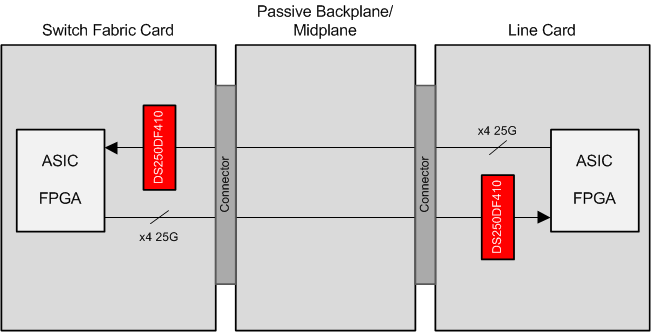
The DS250DF410 has strong equalization capabilities that allow it to recover data over channels up to 35 dB insertion loss. As a result, the optimum placement for the DS250DF410 in a backplane/mid-plane application is with the higher-loss channel segment at the input and the lower-loss channel segment at the output. This reduces the equalization burden on the downstream ASIC/FPGA, as the DS250DF410 is equalizing a majority of the overall channel. This type of asymmetric placement is not a requirement, but when an asymmetric placement is required due to the presence of a passive backplane or mid-plane, then this becomes the recommended placement.
 Figure 23. Backplane/Mid-Plane Application Block Diagram
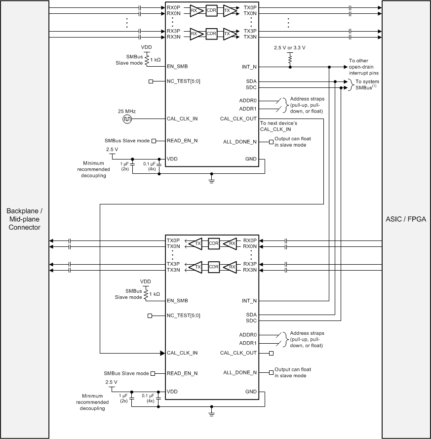
  Figure 24. Backplane/Mid-Plane Application Schematic