SNLS500A July 2016 – January 2024 DS90UB964-Q1
PRODUCTION DATA
- 1
- 1Features
- 2Applications
- 3Description
- Pin Configuration and Functions
-
4Specifications
- 4.1 Absolute Maximum Ratings
- 4.2 ESD Ratings – JEDEC
- 4.3 ESD Ratings – IEC and ISO
- 4.4 Recommended Operating Conditions
- 4.5 Thermal Information
- 4.6 DC Electrical Characteristics
- 4.7 AC Electrical Characteristics
- 4.8 Recommended Timing for the Serial Control Bus
- 4.9 AC Electrical Characteristics
- 4.10 Typical Characteristics
-
5Detailed Description
- 5.1 Overview
- 5.2 Functional Block Diagram
- 5.3 Feature Description
- 5.4
Device Functional Modes
- 5.4.1 RAW Data Type Support and Rates
- 5.4.2 MODE Pin
- 5.4.3 REFCLK
- 5.4.4 Receiver Port Control
- 5.4.5 Input Jitter Tolerance
- 5.4.6 Adaptive Equalizer
- 5.4.7 Channel Monitor Loop-Through Output Driver
- 5.4.8 RX Port Status
- 5.4.9 GPIO Support
- 5.4.10 RAW Mode LV / FV Controls
- 5.4.11 Video Stream Forwarding
- 5.4.12 CSI-2 Protocol Layer
- 5.4.13 CSI-2 Short Packet
- 5.4.14 CSI-2 Long Packet
- 5.4.15 CSI-2 Data Identifier
- 5.4.16 Virtual Channel and Context
- 5.4.17 CSI-2 Mode Virtual Channel Mapping
- 5.4.18 CSI-2 Transmitter Frequency
- 5.4.19 CSI-2 Transmitter Status
- 5.4.20 Video Buffers
- 5.4.21 CSI-2 Line Count and Line Length
- 5.4.22 FrameSync Operation
- 5.4.23
CSI-2 Forwarding
- 5.4.23.1 Best-Effort Round Robin CSI-2 Forwarding
- 5.4.23.2 Synchronized CSI-2 Forwarding
- 5.4.23.3 Basic Synchronized CSI-2 Forwarding
- 5.4.23.4 Line-Interleaved CSI-2 Forwarding
- 5.4.23.5 Line-Concatenated CSI-2 Forwarding
- 5.4.23.6 CSI-2 Replicate Mode
- 5.4.23.7 CSI-2 Transmitter Output Control
- 5.4.23.8 Enabling and Disabling CSI-2 Transmitters
- 5.5
Programming
- 5.5.1 Serial Control Bus
- 5.5.2 Second I2C Port
- 5.5.3 I2C Target Operation
- 5.5.4 Remote Target Operation
- 5.5.5 Remote Target Addressing
- 5.5.6 Broadcast Write to Remote Devices
- 5.5.7 I2C Proxy Controller
- 5.5.8 I2C Proxy Controller Timing
- 5.5.9 Interrupt Support
- 5.5.10 Timestamp – Video Skew Detection
- 5.5.11 Pattern Generation
- 5.5.12 FPD-Link BIST Mode
- 5.6 Register Maps
- 6Application and Implementation
- 7Device and Documentation Support
- 8Revision History
- 9Mechanical, Packaging, and Orderable Information
Package Options
Mechanical Data (Package|Pins)
- RGC|64
Thermal pad, mechanical data (Package|Pins)
- RGC|64
Orderable Information
5.4.7 Channel Monitor Loop-Through Output Driver
The DS90UB964-Q1 includes an internal Channel Monitor Loop-through output on the CMLOUTP/N pins. The CMLOUTP/N pins supply a buffered loop-through output driver to observe the jitter after equalization for each of the four RX receiver channels. The CMLOUT monitors the post EQ stage, thus providing the recovered input of the deserializer signal. The measured serial data width on the CMLOUT loop-through is the total jitter including the internal driver, AEQ, back channel echo, and so forth. Each channel also has a CMLOUT monitor and can be used for debug purposes. This CMLOUT is useful in identifying gross signal conditioning issues.
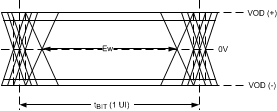
Table 5-7 shows the minimum CMLOUT differential eye opening as a measure of acceptable forward channel signal integrity. A CMLOUT eye opening of at least 0.45 UI suggests that the forward channel signal integrity is likely acceptable. However, further testing such as BIST is recommended to verify error-free operation. An eye opening of less than 0.45 UI indicates possible issues with the forward channel signal integrity.
| PARAMETER | TEST CONDITIONS | PIN | MIN | TYP | MAX | UNIT | |||
|---|---|---|---|---|---|---|---|---|---|
| EW | Differential Output Eye Opening | RL =
100Ω (Figure 5-4) | CMLOUTP, CMLOUTN | 0.45 | UI(1) | ||||
10-bit mode: 1 UI = 1 / ( 28 x PCLK / 2 )
RAW 12-bit HF mode: 1 UI = 1 / ( 28 x 2/3 x PCLK )
RAW 12-bit LF mode: 1 UI = 1 / ( 28 x PCLK )
 Figure 5-4 CMLOUT Output Driver
Table 5-8 includes details on selecting the corresponding RX receiver of CMLOUTP/N configuration.
| FPD3 RX Port 0 | FPD3 RX Port 1 | FPD3 RX Port 2 | FPD3 RX Port 3 | |
|---|---|---|---|---|
| ENABLE MAIN LOOPTHRU DRIVER | 0xB0 = 0x14 0xB1 = 0x00 0xB2 = 0x80 | 0xB0 = 0x14 0xB1 = 0x00 0xB2 = 0x80 | 0xB0 = 0x14 0xB1 = 0x00 0xB2 = 0x80 | 0xB0 = 0x14 0xB1 = 0x00 0xB2 = 0x80 |
| SELECT CHANNEL MUX | 0xB1 = 0x01 0xB2 = 0x01 | 0xB1 = 0x01 0xB2 = 0x02 | 0xB1 = 0x01 0xB2 = 0x04 | 0xB1 = 0x01 0xB2 = 0x08 |
| SELECT RX PORT | 0xB0 = 0x04 0xB1 = 0x0F 0xB2 = 0x01 0xB1 = 0x10 0xB2 = 0x02 | 0xB0 = 0x08 0xB1 = 0x0F 0xB2 = 0x01 0xB1 = 0x10 0xB2 = 0x02 | 0xB0 = 0x0C 0xB1 = 0x0F 0xB2 = 0x01 0xB1 = 0x10 0xB2 = 0x02 | 0xB0 = 0x10 0xB1 = 0x0F 0xB2 = 0x01 0xB1 = 0x10 0xB2 = 0x02 |