SLASE82B June 2015 – March 2024 HD3SS3411-Q1
PRODUCTION DATA
- 1
- 1 Features
- 2 Applications
- 3 Description
- 4 Pin Configuration and Functions
- 5 Specifications
- 6 Detailed Description
- 7 Application and Implementation
- 8 Device and Documentation Support
- 9 Revision History
- 10Mechanical, Packaging, and Orderable Information
Package Options
Mechanical Data (Package|Pins)
- RWA|14
Thermal pad, mechanical data (Package|Pins)
Orderable Information
4 Pin Configuration and Functions
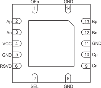
 Figure 4-1 RWA Package, 14-Pin WQFN (Top View)
Table 4-1 Pin Functions
| NAME | NO | TYPE(1) | DESCRIPTION |
|---|---|---|---|
| Ap | 2 | I/O | Port A, High Speed Positive Signal |
| An | 3 | I/O | Port A, High Speed Negative Signal |
| Bp | 13 | I/O | Port B, High Speed Positive Signal |
| Bn | 12 | I/O | Port B, High Speed Negative Signal |
| Cp | 10 | I/O | Port C, High Speed Positive Signal |
| Cn | 9 | I/O | Port C, High Speed Negative Signal |
| GND | 5,8,11,14, Pad | G | Ground |
| OEn | 1 | I | Active Low Chip Enable L: Normal operation H: Shutdown |
| RSVD | 6 | I/O | Reserved Pin – connect or pulldown to GND |
| SEL | 7 | I | Port select pin L: Port A to Port B H: Port A to Port C |
| VCC | 4 | P | 3.3V power |
(1) The high speed data ports incorporate 20kΩ pulldown resistors
that are switched in when a port is not selected and switched out when the port
is selected..