SLLS983L June 2009 – October 2023 ISO1050
PRODUCTION DATA
- 1
- 1 Features
- 2 Applications
- 3 Description
- 4 Revision History
- 5 Pin Configuration and Functions
-
6 Specifications
- 6.1 Absolute Maximum Ratings
- 6.2 ESD Ratings
- 6.3 Recommended Operating Conditions
- 6.4 Thermal Information
- 6.5 Power Ratings
- 6.6 Insulation Specifications
- 6.7 Safety-Related Certifications
- 6.8 Safety Limiting Values
- 6.9 Electrical Characteristics - DC Specification
- 6.10 Switching Characteristics
- 6.11 Insulation Characteristics Curves
- 6.12 Typical Characteristics
- 7 Parameter Measurement Information
- 8 Detailed Description
- 9 Application and Implementation
- 10Power Supply Recommendations
- 11Layout
- 12Device and Documentation Support
- 13Mechanical, Packaging, and Orderable Information
Package Options
Mechanical Data (Package|Pins)
Thermal pad, mechanical data (Package|Pins)
Orderable Information
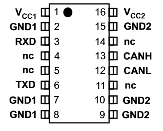
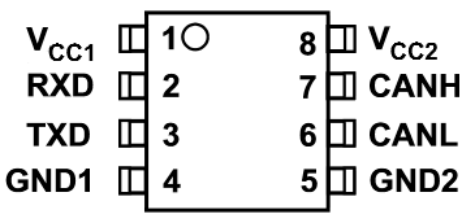
5 Pin Configuration and Functions
 Figure 5-1 16-PinDW
PackageTop View
 Figure 5-2 8-PinDUB
PackageTop View
Figure 5-2 8-PinDUB
PackageTop ViewTable 5-1 Pin Functions
| PIN | TYPE | DESCRIPTION | ||
|---|---|---|---|---|
| NAME | DW | DUB | ||
| VCC1 | 1 | 1 | Supply | Digital-side supply voltage (3 to 5.5 V) |
| GND1 | 2 | — | Ground | Digital-side ground connection |
| RXD | 3 | 2 | O | CAN receive data output (LOW for dominant and HIGH for recessive bus states) |
| NC | 4 | — | NC | No connect |
| NC | 5 | — | NC | No connect |
| TXD | 6 | 3 | I | CAN transmit data input (LOW for dominant and HIGH for recessive bus states) |
| GND1 | 7 | 4 | Ground | Digital-side ground connection |
| GND1 | 8 | — | Ground | Digital-side ground connection |
| GND2 | 9 | 5 | Ground | Transceiver-side ground connection |
| GND2 | 10 | — | Ground | Transceiver-side ground connection |
| NC | 11 | — | NC | No connect |
| CANL | 12 | 6 | I/O | Low-level CAN bus line |
| CANH | 13 | 7 | I/O | High-level CAN bus line |
| NC | 14 | — | NC | No connect |
| GND2 | 15 | — | Ground | Transceiver-side ground connection |
| VCC2 | 16 | 8 | Supply | Transceiver-side supply voltage (5 V) |