SNOSCZ7B December 2015 – April 2024 LDC0851
PRODUCTION DATA
- 1
- 1 Features
- 2 Applications
- 3 Description
- 4 Pin Configuration and Functions
- 5 Specifications
- 6 Detailed Description
- 7 Application and Implementation
- 8 Device and Documentation Support
- 9 Revision History
- 10Mechanical, Packaging, and Orderable Information
Package Options
Mechanical Data (Package|Pins)
- DSG|8
Thermal pad, mechanical data (Package|Pins)
- DSG|8
Orderable Information
6.3.3 Setting the Threshold Adjust Values
To configure a threshold setting, connect a 49.9 kΩ resistor (R1) between VDD and the ADJ pin as shown in Figure 6-4. The threshold is determined by the value of R2 as shown in the Table 6-1 below. R1 and R2 should be 1% or tighter tolerance resistors with a temperature coefficient of <50 ppm/°C.
| ADJ Code | R2 (kΩ) |
|---|---|
| 1 | 3.32 |
| 2 | 5.11 |
| 3 | 7.15 |
| 4 | 9.31 |
| 5 | 11.5 |
| 6 | 14 |
| 7 | 16.5 |
| 8 | 19.6 |
| 9 | 22.6 |
| 10 | 26.1 |
| 11 | 30.1 |
| 12 | 34 |
| 13 | 39 |
| 14 | 44.2 |
| 15 | 49.9 |
The switching distance for each ADJ code can be approximated with the following formula:
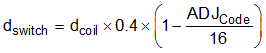
where:
- dswitch is the approximated switching distance threshold
- dcoil is the coil diameter, in the same units as dswitch
- ADJCode is the desired value from Table 6-1
For example, consider a coil with a diameter of 10 mm: An ADJ code of 1 will yield a switching distance of 3.75 mm and for a code of 15 a switching distance of 0.25 mm. This method helps reduce the effort needed to design the coil ratio precisely for a specific switching distance. It should be noted that the maximum sensing distance is determined almost entirely by the diameter of the coil for circular coils or by the minimum outer dimension for rectangular coils.