SNOS412Q February 2000 – January 2023 LM1117
PRODUCTION DATA
- 1 Features
- 2 Applications
- 3 Description
- 4 Revision History
- 5 Device Comparison Table
- 6 Pin Configuration and Functions
- 7 Specifications
- 8 Detailed Description
- 9 Application and Implementation
- 10Device and Documentation Support
- 11Mechanical, Packaging, and Orderable Information
Package Options
Mechanical Data (Package|Pins)
Thermal pad, mechanical data (Package|Pins)
- KTT|3
Orderable Information
3 Description
The LM1117 is a low dropout voltage regulator with a dropout of 1.2 V at 800 mA of load current.
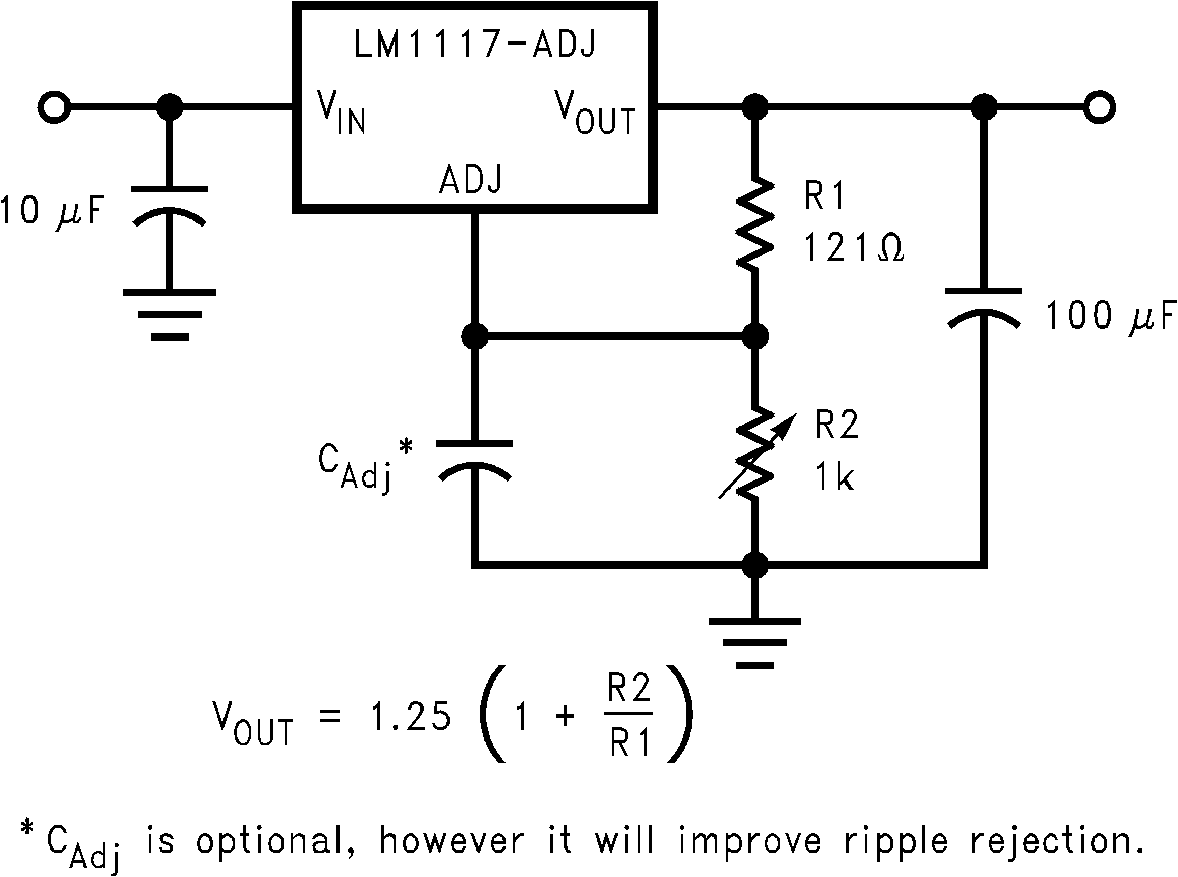
The LM1117 is available in an adjustable version, which can set the output voltage from 1.25 V to 13.8 V with only two external resistors. In addition, the device is available in five fixed voltages, 1.8 V, 2.5 V, 3.3 V, and 5 V.
The LM1117 offers current limiting and thermal shutdown. The circuit includes a Zener trimmed band-gap reference to assure output voltage accuracy to within ±1%.
A minimum of 10-µF tantalum capacitor is required at the output to improve the transient response and stability.
| PART NUMBER | PACKAGE(1) | BODY SIZE (NOM) |
|---|---|---|
| LM1117, LM1117I |
DCY (SOT-223, 4) | 6.50 mm × 3.50 mm |
| NDE (TO-220, 3) | 14.986 mm × 10.16 mm | |
| NDP (TO-252, 3) | 6.58 mm × 6.10 mm | |
| NGN (WSON, 8) | 4.00 mm × 4.00 mm | |
| KTT (TO-263, 3) | 10.18 mm × 8.41 mm |
 Adjustable Output Regulator