SNVS118F december 1999 – may 2023 LM2594 , LM2594HV
PRODUCTION DATA
- 1
- 1 Features
- 2 Applications
- 3 Description
- 4 Revision History
- 5 Description (continued)
- 6 Pin Configuration and Functions
-
7 Specifications
- 7.1 Absolute Maximum Ratings
- 7.2 ESD Ratings
- 7.3 Recommended Operating Conditions
- 7.4 Thermal Information
- 7.5 Electrical Characteristics – 3.3 V
- 7.6 Electrical Characteristics – 5 V
- 7.7 Electrical Characteristics – 12 V
- 7.8 Electrical Characteristics – Adjustable
- 7.9 Electrical Characteristics – All Output Voltage Versions
- 7.10 Typical Characteristics
- 8 Detailed Description
- 9 Application and Implementation
- 10Device and Documentation Support
- 11Mechanical, Packaging, and Orderable Information
Package Options
Mechanical Data (Package|Pins)
Thermal pad, mechanical data (Package|Pins)
Orderable Information
9.1.5 Output Voltage Ripple and Transients
The output voltage of a switching power supply operating in the continuous mode contains a sawtooth ripple voltage at the switcher frequency, and can also contain short voltage spikes at the peaks of the sawtooth waveform.
The output ripple voltage is a function of the inductor sawtooth ripple current and the ESR of the output capacitor. A typical output ripple voltage can range from approximately 0.5% to 3% of the output voltage. To obtain low ripple voltage, the ESR of the output capacitor must be low; however, caution must be exercised when using extremely low ESR capacitors because they can affect the loop stability, resulting in oscillation problems. If very low output ripple voltage is needed (less than 15 mV), TI recommends a post ripple filter (see Figure 9-13). The inductance required is typically between 1 μH and 5 μH, with low DC resistance, to maintain good load regulation. A low ESR output filter capacitor is also required to assure good dynamic load response and ripple reduction. The ESR of this capacitor can be as low as desired, because it is out of the regulator feedback loop. Figure 8-9 shows a typical output ripple voltage, with and without a post ripple filter.
When observing output ripple with a scope, it is essential that a short, low inductance scope probe ground connection be used. Most scope probe manufacturers provide a special probe terminator which is soldered onto the regulator board, preferably at the output capacitor. This provides a very short scope ground, thus eliminating the problems associated with the three-inch ground lead normally provided with the probe, and provides a much cleaner and more accurate picture of the ripple voltage waveform.
The voltage spikes are caused by the fast switching action of the output switch and the diode, the parasitic inductance of the output filter capacitor, and its associated wiring. To minimize these voltage spikes, the output capacitor must be designed for switching regulator applications, and the lead lengths must be kept very short. Wiring inductance, stray capacitance, as well as the scope probe used to evaluate these transients, all contribute to the amplitude of these spikes.
When a switching regulator is operating in the continuous mode, the inductor current waveform ranges from a triangular to a sawtooth type of waveform (depending on the input voltage). For a given input and output voltage, the peak-to-peak amplitude of this inductor current waveform remains constant. As the load current increases or decreases, the entire sawtooth current waveform also rises and falls. The average value (or the center) of this current waveform is equal to the DC load current.
If the load current drops to a low enough level, the bottom of the sawtooth current waveform reaches zero, and the switcher smoothly changes from a continuous to a discontinuous mode of operation. Most switcher designs (regardless how large the inductor value is) is forced to run discontinuous if the output is lightly loaded. This is a perfectly acceptable mode of operation.
 Figure 9-9 Peak-to-Peak Inductor Ripple Current vs Load Current
In a switching regulator design, knowing the value of the peak-to-peak inductor ripple current (ΔIIND) can be useful for determining a number of other circuit parameters. Parameters such as, peak inductor or peak switch current, minimum load current before the circuit becomes discontinuous, output ripple voltage and output capacitor ESR can all be calculated from the peak-to-peak ΔIIND. When the inductor nomographs shown in Figure 9-5 through Figure 9-8 are used to select an inductor value, the peak-to-peak inductor ripple current can immediately be determined. Figure 9-9 shows the range of (ΔIIND) that can be expected for different load currents. Figure 9-9 also shows how the peak-to-peak inductor ripple current (ΔIIND) changes as the designer goes from the lower border to the upper border (for a given load current) within an inductance region. The upper border represents a higher input voltage, while the lower border represents a lower input voltage (see Section 9.1.4).
These curves are only correct for continuous mode operation, and only if the inductor selection guides are used to select the inductor value.
Consider the following example:
VOUT = 5 V, maximum load current of 300 mA
VIN = 15 V, nominal, varying between 11 V and 20 V
The selection guide in Figure 9-6 shows that the vertical line for a 0.3-A load current and the horizontal line for the 15-V input voltage intersect approximately midway between the upper and lower borders of the 150-μH inductance region. A 150-μH inductor allows a peak-to-peak inductor current (ΔIIND) to flow a percentage of the maximum load current. Referring to Figure 9-9, follow the 0.3-A line approximately midway into the inductance region, and read the peak-to-peak inductor ripple current (ΔIIND) on the left hand axis (approximately 150 mAp-p).
As the input voltage increases to 20 V, it approaches the upper border of the inductance region, and the inductor ripple current increases. Figure 9-9 shows that for a load current of 0.3 A, the peak-to-peak inductor ripple current (ΔIIND) is 150 mA with 15V in, and can range from 175 mA at the upper border (20 V in) to 120 mA at the lower border (11 V in).
After the ΔIIND value is known, the following formulas can be used to calculate additional information about the switching regulator circuit.
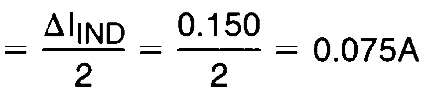
- Peak Inductor or peak switch current
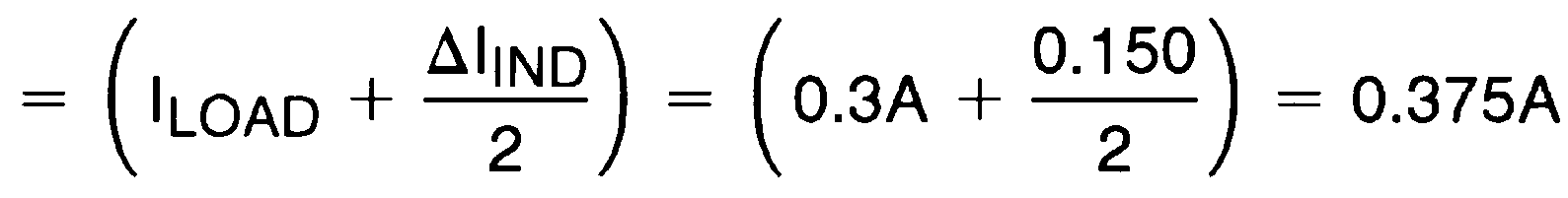
- Minimum load current before the circuit becomes discontinuous
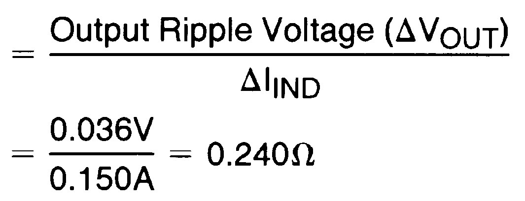
- Output Ripple Voltage
- = (ΔIIND) × (ESR of COUT)
- = 0.150 A × 0.240 Ω = 36 mVp-p
- or
- ESR of COUT