SNVS325E January 2005 – January 2016 LM2852
PRODUCTION DATA.
- 1 Features
- 2 Applications
- 3 Description
- 4 Revision History
- 5 Pin Configuration and Functions
- 6 Specifications
- 7 Detailed Description
- 8 Application and Implementation
- 9 Power Supply Recommendations
- 10Layout
- 11Device and Documentation Support
- 12Mechanical, Packaging, and Orderable Information
Package Options
Mechanical Data (Package|Pins)
- PWP|14
Thermal pad, mechanical data (Package|Pins)
- PWP|14
Orderable Information
7 Detailed Description
7.1 Overview
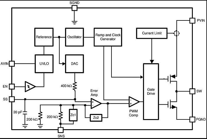
The LM2852 is a DC-DC synchronous buck regulator. Integration of the PWM controller, power switches and compensation network greatly reduces the component count required to implement a switching power supply.
7.2 Functional Block Diagram

7.3 Feature Description
7.3.1 Split-Rail Operation
The LM2852 can be powered using two separate voltages for AVIN and PVIN. AVIN is the supply for the control logic; PVIN is the supply for the power FETs. The output filter components need to be chosen based on the value of PVIN. For PVIN levels lower than 3.3 V, use output filter component values recommended for 3.3 V. PVIN must always be equal to or less than AVIN.
 Figure 11. Split-Rail Operation
7.3.2 Switch Node Protection
The LM2852 includes protection circuitry that monitors the voltage on the switch pin. Under certain conditions, switching is disabled in order to protect the switching devices. One result of the protection circuitry may be observed when power to the LM2852 is applied with no or light load on the output. The output regulates to the rated voltage, but no switching may be observed. As soon as the output is loaded, the LM2852 begins normal switching operation.
7.4 Device Functional Modes
The LM2852 Enable pin is internally pulled up so that the part is enabled anytime the input voltage exceeds the UVLO threshold. A pulldown resistor can be used to set the enable input to low.