SNVS325E January 2005 – January 2016 LM2852
PRODUCTION DATA.
- 1 Features
- 2 Applications
- 3 Description
- 4 Revision History
- 5 Pin Configuration and Functions
- 6 Specifications
- 7 Detailed Description
- 8 Application and Implementation
- 9 Power Supply Recommendations
- 10Layout
- 11Device and Documentation Support
- 12Mechanical, Packaging, and Orderable Information
Package Options
Mechanical Data (Package|Pins)
- PWP|14
Thermal pad, mechanical data (Package|Pins)
- PWP|14
Orderable Information
10 Layout
10.1 Layout Guidelines
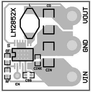
These are several guidelines to follow while designing the PCB layout for an LM2852 application.
- The input bulk capacitor, CIN, must be placed very close to the PVIN pin to keep the resistance as low as possible between the capacitor and the pin. High-current levels are present in this connection
- All ground connections must be tied together. Use a broad ground plane, for example a completely filled back plane, to establish the lowest resistance possible between all ground connections
- The sense pin connection must be made as close to the load as possible so that the voltage at the load is the expected regulated value. The sense line must not run too close to nodes with high EMI (such as the switch node) to minimize interference
- The switch node connections must be low resistance to reduce power losses. Low resistance means the trace between the switch pin and the inductor must be wide. However, the area of the switch node must not be too large since EMI increases with greater area. So connect the inductor to the switch pin with a short, but wide trace. Other high current connections in the application such as PVIN and VOUT assume the same trade off between low resistance and EMI
- Allow area under the chip to solder the entire exposed die attach pad to ground for improved thermal and electrical performance
10.2 Layout Example
 Figure 15. PCB Layout Example