SNVS325E January 2005 – January 2016 LM2852
PRODUCTION DATA.
- 1 Features
- 2 Applications
- 3 Description
- 4 Revision History
- 5 Pin Configuration and Functions
- 6 Specifications
- 7 Detailed Description
- 8 Application and Implementation
- 9 Power Supply Recommendations
- 10Layout
- 11Device and Documentation Support
- 12Mechanical, Packaging, and Orderable Information
Package Options
Mechanical Data (Package|Pins)
- PWP|14
Thermal pad, mechanical data (Package|Pins)
- PWP|14
Orderable Information
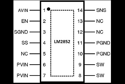
5 Pin Configuration and Functions
PWP Package
14-Pin HTSSOP
Top View

Pin Functions
| PIN | I/O | DESCRIPTION | |
|---|---|---|---|
| NAME | NO. | ||
| AVIN | 1 | I | Chip bias input pin. This provides power to the logic of the chip. Connect to the input voltage or a separate rail. |
| EN | 2 | I | Enable. Connect this pin to ground to disable the chip; connect to AVIN or leave floating to enable the chip; enable is internally pulled up. |
| Exposed | Connect to ground. | ||
| NC | 5, 12, 13 | No connect. These pins must be tied to ground or left floating in the application. | |
| PGND | 10, 11 | G | Power ground. Connect this to an internal ground plane or other large ground plane. |
| PVIN | 6, 7 | I | Input supply pin. PVIN is connected to the input voltage. This rail connects to the source of the internal power PFET. |
| SGND | 3 | G | Signal ground. |
| SNS | 14 | O | Output voltage sense pin. Connect this pin to the output voltage as close to the load as possible. |
| SS | 4 | I | Soft-start pin. Connect this pin to a small capacitor to control startup. The soft-start capacitance range is restricted to values 1 nF to 50 nF. |
| SW | 8, 9 | O | Switch pin. Connect to the output inductor. |