SNVS099I May 1999 – October 2016 LM2991
PRODUCTION DATA.
- 1 Features
- 2 Applications
- 3 Description
- 4 Revision History
- 5 Pin Configuration and Functions
- 6 Specifications
- 7 Detailed Description
- 8 Application and Implementation
- 9 Power Supply Recommendations
- 10Layout
- 11Device and Documentation Support
- 12Mechanical, Packaging, and Orderable Information
Package Options
Mechanical Data (Package|Pins)
Thermal pad, mechanical data (Package|Pins)
- KTT|5
Orderable Information
7 Detailed Description
7.1 Overview
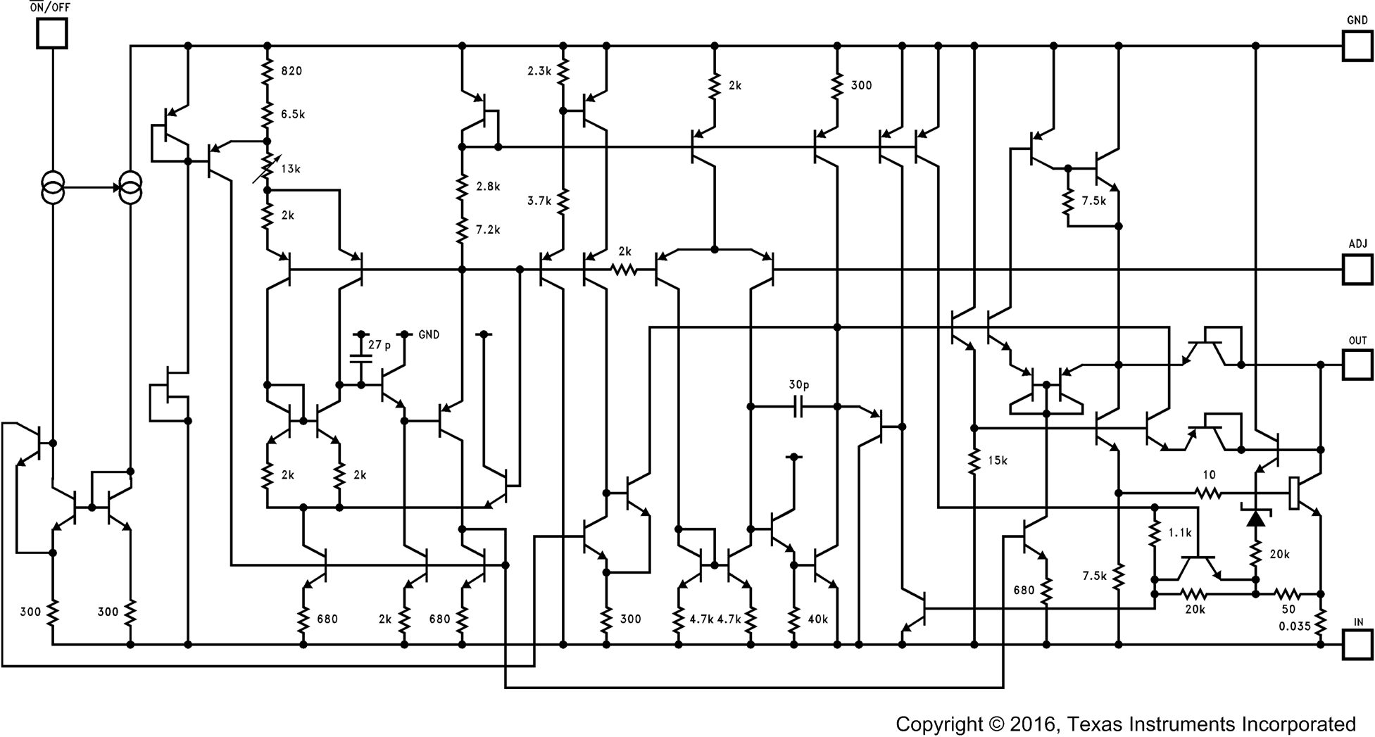
The LM2991 is a five-pin, low-dropout, 1-A negative adjustable voltage regulator and negative power supply, ideally suited for a dual-supply system when using together with LM2941 series. The device may also be used as an adjustable current-sink load.
7.2 Functional Block Diagram

7.3 Feature Description
7.3.1 ON/Off Pin
The LM2991 regulator can be turned off by applying a TTL or CMOS level high signal to the ON/OFF pin. The impedance of the voltage source driving the ON/OFF pin must be low enough to source the ON/OFF pin input current to meet the OFF threshold voltage level, 100 µA maximum at 2.4 V.
If the ON/OFF function is not needed, connect the pin to GND. The ON/OFF pin should not be left floating, as this is not an ensured operating condition. See Figure 15.
7.3.2 Forcing The Output Positive
Due to an internal clamp circuit, the LM2991 can withstand positive voltages on its output. If the voltage source pulling the output positive is DC, the current must be limited to 1.5 A. A current over 1.5 A fed back into the LM2991 could damage the device. The LM2991 output can also withstand fast positive voltage transients up to 26 V, without any current limiting of the source. However, if the transients have a duration of over 1 ms, the output should be clamped with a Schottky diode to ground.
7.3.3 Thermal Shutdown
The LM2991 has an internally set thermal shutdown point of typically 160°C, with approximately 10°C of hysteresis. This thermal shutdown temperature point is outside the specified Recommended Operating Conditions range, above the Absolute Maximum Ratings, and is intended as a safety feature for momentary fault conditions only. Avoid continuous operation near the thermal shutdown temperature as it may have a negative affect on the life of the device.
7.4 Device Functional Modes
7.4.1 Operation with VOUT(TARGET) –5 V ≥ VIN > –26 V
The device operates if the input voltage is within VOUT(TARGET) –5 V to –26 V range. At input voltages beyond the VIN requirement, the devices do not operate correctly, and output voltage may not reach target value.