SNVS099I May 1999 – October 2016 LM2991
PRODUCTION DATA.
- 1 Features
- 2 Applications
- 3 Description
- 4 Revision History
- 5 Pin Configuration and Functions
- 6 Specifications
- 7 Detailed Description
- 8 Application and Implementation
- 9 Power Supply Recommendations
- 10Layout
- 11Device and Documentation Support
- 12Mechanical, Packaging, and Orderable Information
Package Options
Mechanical Data (Package|Pins)
Thermal pad, mechanical data (Package|Pins)
- KTT|5
Orderable Information
8 Application and Implementation
NOTE
Information in the following applications sections is not part of the TI component specification, and TI does not warrant its accuracy or completeness. TI’s customers are responsible for determining suitability of components for their purposes. Customers should validate and test their design implementation to confirm system functionality.
8.1 Application Information
The LM2991 is a 1-A negative adjustable voltage regulator with an operating VIN range of –6 V to –26 V, and a regulated VOUT having 5% accuracy with a maximum rated IOUT current of 1 A. Efficiency is defined by the ratio of output voltage to input voltage because the LM2991 is a linear voltage regulator. To achieve high efficiency, the dropout voltage (VIN – VOUT) must be as small as possible, thus requiring a very low dropout LDO.
Successfully implementing an LDO in an application depends on the application requirements. If the requirements are simply input voltage and output voltage, compliance specifications (such as internal power dissipation or stability) must be verified to ensure a solid design. If timing, start-up, noise, PSRR, or any other transient specification is required, the design becomes more challenging.
8.2 Typical Application
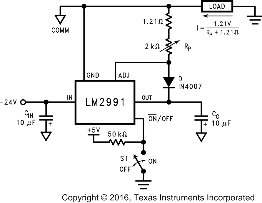 Figure 15. LM2991 Typical Application With Adjustable Current Sink
8.2.1 Design Requirements
For this design example, use the parameters listed in Table 1 as the input parameters.
Table 1. Design Parameters
| DESIGN PARAMETER | DESIGN REQUIREMENT |
|---|---|
| Input voltage | –26 V to –5 V |
| Output voltage | –2 V to –25 V (typical) |
| Output current | up to 1 A |
8.2.2 Detailed Design Procedure
At 400-mA loading, the dropout of the LM2991 has 1-V maximum dropout over temperature, thus an –5 V headroom is sufficient for operation over both input and output voltage accuracy. The efficiency of the LM2991 in this configuration is VOUT / VIN = 50%.
To achieve the smallest form factor, the TO-263 (KTT) package is selected. Select input and output capacitors in accordance with the External Capacitors section. Aluminum capacitances of 470 μF for the input and 50-μF capacitors for the output are selected. With an efficiency of 50% and a 400-mA maximum load, the internal power dissipation is 2000 mW, which corresponds to 82.5°C junction temperature rise for the TO-263 package. With an 25°C ambient temperature, the junction temperature is at 107.5°C.
8.2.2.1 External Capacitors
The LM2991 regulator requires an output capacitor to maintain stability. The capacitor must be at least 10-μF aluminum electrolytic or 1-μF solid tantalum. The equivalent series resistance (ESR) of the output capacitor must be less than 10 Ω, or the zero added to the regulator frequency response by the ESR could reduce the phase margin, creating oscillations. An input capacitor, of at least 1-μF solid tantalum or 10-μF aluminum electrolytic, is also needed if the regulator is situated more than 6 inches from the input power supply filter.
8.2.2.1.1 Input Capacitor
TI recommends a solid tantalum or ceramic capacitor whose value is at least 1 μF, but an aluminum electrolytic (≥ 10 μF) may be used. However, aluminum electrolytic types should not be used in applications where the ambient temperature can drop below 0°C because their internal impedance increases significantly at cold temperatures.
8.2.2.1.2 Output Capacitor
The output capacitor must meet the ESR limits shown in Figure 16, which means it must have an ESR between about 25 mΩ and 10 Ω.
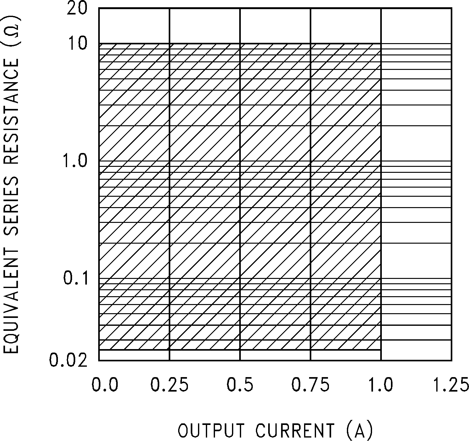 Figure 16. Output Capacitor ESR Range
A solid tantalum (value ≥ 1 µF) is the best choice for the output capacitor. An aluminum electrolytic (≥ 10 µF) may be used if the ESR is in the stable range.
It should be noted that the ESR of a typical aluminum electrolytic will increase by as much as 50× as the temperature is reduced from 25°C down to −40°C, while a tantalum exhibits an ESR increase of about 2× over the same range. For this and other reasons, aluminum electrolytics should not be used in applications where low operating temperatures occur.
The lower stable ESR limit of 25 mΩ means that ceramic capacitors can not be used directly on the output of an LDO. A ceramic (≥ 2.2 µF) can be used on the output if some external resistance is placed in series with it (1 Ω recommended). Dielectric types X7R or X5R must be used if the temperature range of the application varies more than ± 25° from ambient to assure the amount of capacitance is sufficient.
8.2.2.2 Ceramic Bypass Capacitors
Many designers place distributed ceramic capacitors whose value is in the range of 1000 pF to 0.1 µF at the power input pins of the IC's across a circuit board. These can cause reduced phase margin or oscillations in LDO regulators.
The advent of multi-layer boards with dedicated power and ground planes has removed the trace inductance that (previously) provided the necessary "de-coupling" to shield the output of the LDO from the effects of bypass capacitors.
Avoid these capacitors, if possible; if ceramic bypass capacitors are used, keep them as far away from the LDO output as is practical.
8.2.2.3 Minimum Load
A minimum load current of 500 μA is required for proper operation. The external resistor divider can provide the minimum load, with the resistor from the adjust pin to ground set to 2.4 kΩ.
8.2.2.4 Setting The Output Voltage
The output voltage of the LM2991 is set externally by a resistor divider using Equation 1:
where
- VREF = −1.21 V
The output voltage can be programmed within the range of −3 V to −24 V, typically an even greater range of −2 V to −25 V. The adjust pin current is about 60 nA, causing a slight error in the output voltage. However, using resistors lower than 100 kΩ makes the error due to the adjust pin current negligible. For example, neglecting the adjust pin current, and setting R2 to 100 kΩ and VOUT to −5 V, results in an output voltage error of only 0.16%.
8.2.2.5 Power Dissipation
Knowing the device power dissipation and proper sizing of the thermal plane connected to the thermal tab is critical to ensuring reliable operation. Device power dissipation depends on input voltage, output voltage, and load conditions and can be calculated with Equation 2.
Power dissipation can be minimized, and greater efficiency can be achieved, by using the lowest available voltage drop option that would still be greater than the dropout voltage (VDO). However, keep in mind that higher voltage drops result in better dynamic (that is, PSRR and transient) performance.
Power dissipation and junction temperature are most often related by the junction-to-ambient thermal resistance (RθJA) of the combined PCB and device package and the temperature of the ambient air (TA), according to Equation 3 or Equation 4:
Unfortunately, this RθJA is highly dependent on the heat-spreading capability of the particular PCB design, and therefore varies according to the total copper area, copper weight, and location of the planes. The RθJA recorded in Thermal Information is determined by the specific EIA/JEDEC JESD51-7 standard for PCB and copper-spreading area, and is to be used only as a relative measure of package thermal performance. For a well-designed thermal layout, RθJA is actually the sum of the package junction-to-case (bottom) thermal resistance (RθJCbot) plus the thermal resistance contribution by the PCB copper area acting as a heat sink.
8.2.2.6 Estimating Junction Temperature
The EIA/JEDEC standard recommends the use of psi (Ψ) thermal characteristics to estimate the junction temperatures of surface mount devices on a typical PCB board application. These characteristics are not true thermal resistance values, but rather package specific thermal characteristics that offer practical and relative means of estimating junction temperatures. These psi metrics are determined to be significantly independent of copper-spreading area. The key thermal characteristics (ΨJT and ΨJB) are given in Thermal Information and are used in accordance with Equation 5 or Equation 6.
where
- PD(MAX) is explained in Equation 4
- TTOP is the temperature measured at the center-top of the device package.
where
- PD(MAX) is explained in Equation 4
- TBOARD is the PCB surface temperature measured 1-mm from the device package and centered on the package edge.
For more information about the thermal characteristics ΨJT and ΨJB, see Semiconductor and IC Package Thermal Metrics; for more information about measuring TTOP and TBOARD, see Using New Thermal Metrics; and for more information about the EIA/JEDEC JESD51 PCB used for validating RθJA, see Thermal Characteristics of Linear and Logic Packages Using JEDEC PCB Designs. These application notes are available at www.ti.com..
8.2.3 Application Curves
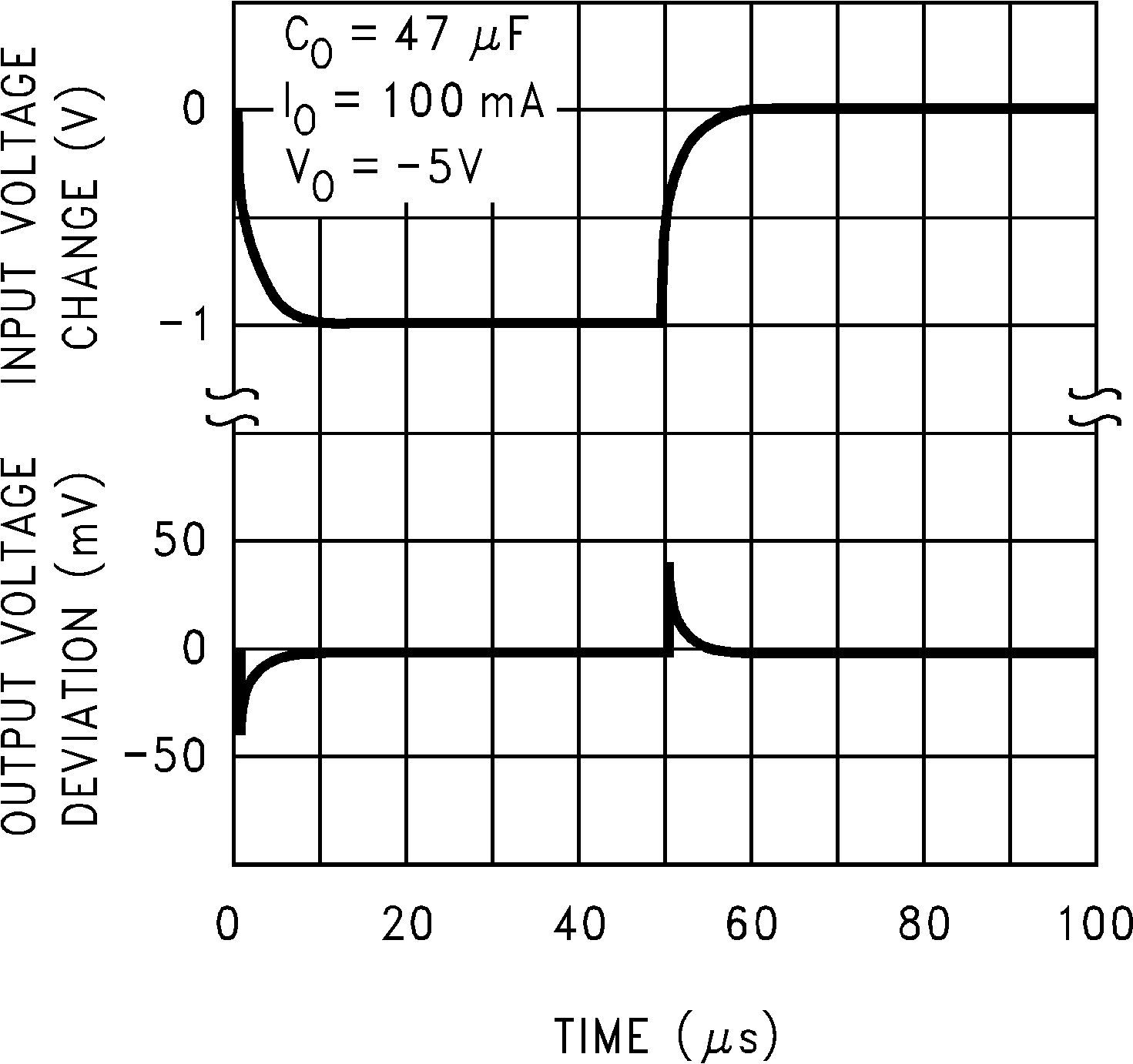
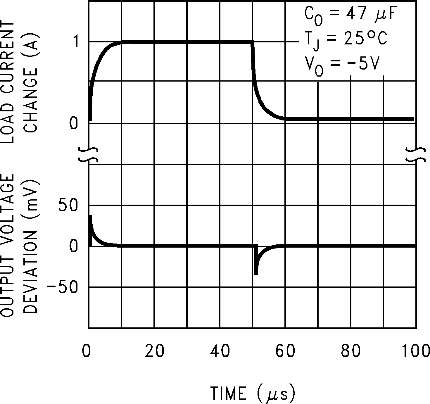
8.2.4 Additional Application Circuits
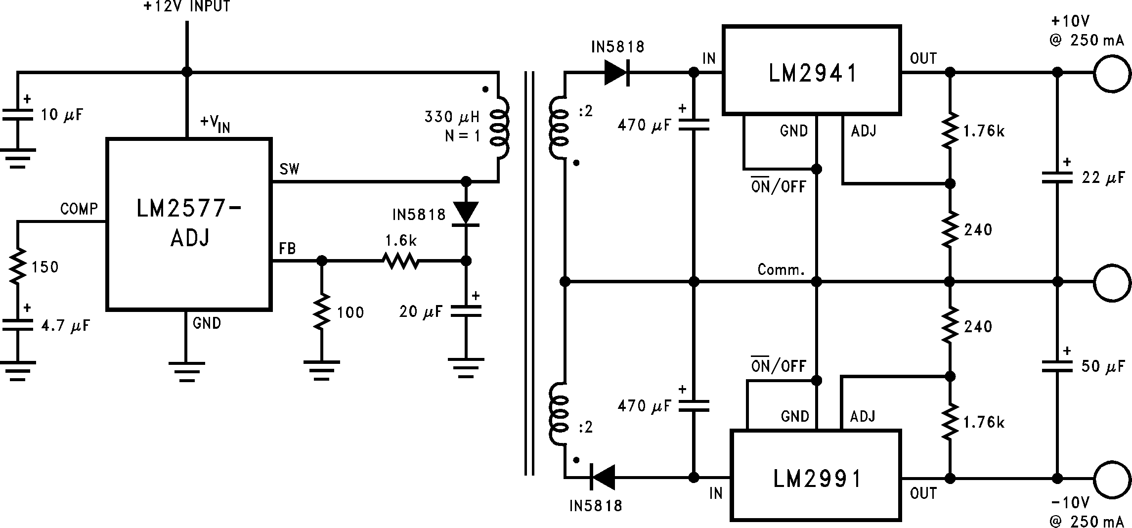 Figure 19. Fully Isolated Post-Switcher Regulator