SNVSCL9 March 2011 – November 2023 LM3481-Q1
PRODUCTION DATA
- 1
- 1 Features
- 2 Applications
- 3 Description
- 4 Pin Configuration and Functions
- 5 Specifications
- 6 Detailed Description
-
7 Application and Implementation
- 7.1 Application Information
- 7.2
Typical Applications
- 7.2.1
Boost Converter
- 7.2.1.1 Design Requirements
- 7.2.1.2
Detailed Design Procedure
- 7.2.1.2.1 Custom Design with WEBENCH Tools
- 7.2.1.2.2 Power Inductor Selection
- 7.2.1.2.3 Programming the Output Voltage and Output Current
- 7.2.1.2.4 Current Limit With Additional Slope Compensation
- 7.2.1.2.5 Power Diode Selection
- 7.2.1.2.6 Power MOSFET Selection
- 7.2.1.2.7 Input Capacitor Selection
- 7.2.1.2.8 Output Capacitor Selection
- 7.2.1.2.9 Driver Supply Capacitor Selection
- 7.2.1.2.10 Compensation
- 7.2.1.3 Application Curve
- 7.2.2 Typical SEPIC Converter
- 7.2.1
Boost Converter
- 7.3 Power Supply Recommendations
- 7.4 Layout
- 8 Device and Documentation Support
- 9 Revision History
- 10Mechanical, Packaging, and Orderable Information
Package Options
Mechanical Data (Package|Pins)
- DGS|10
Thermal pad, mechanical data (Package|Pins)
Orderable Information
7.2.2.2.5 SEPIC Capacitor Selection
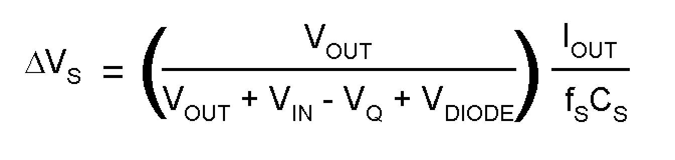
The selection of SEPIC capacitor, CS, depends on the rms current. The rms current of the SEPIC capacitor is given by:

The SEPIC capacitor must be rated for a large ACrms current relative to the output power. This property makes the SEPIC much better suited to lower power applications where the rms current through the capacitor is small (relative to capacitor technology). The voltage rating of the SEPIC capacitor must be greater than the maximum input voltage. Tantalum capacitors are the best choice for SMT, having high rms current ratings relative to size. Ceramic capacitors could be used, but the low C values will tend to cause larger changes in voltage across the capacitor due to the large currents, and high C value ceramics are expensive. Electrolytic capacitors work well for through hole applications where the size required to meet the rms current rating can be accommodated. There is an energy balance between CS and L1, which can be used to determine the value of the capacitor. The basic energy balance equation is:
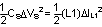
Where
is the ripple voltage across the SEPIC capacitor, and

is the ripple current through the inductor L1. The energy balance equation can be solved to provide a minimum value for CS:
