SNVSCL9 March 2011 – November 2023 LM3481-Q1
PRODUCTION DATA
- 1
- 1 Features
- 2 Applications
- 3 Description
- 4 Pin Configuration and Functions
- 5 Specifications
- 6 Detailed Description
-
7 Application and Implementation
- 7.1 Application Information
- 7.2
Typical Applications
- 7.2.1
Boost Converter
- 7.2.1.1 Design Requirements
- 7.2.1.2
Detailed Design Procedure
- 7.2.1.2.1 Custom Design with WEBENCH Tools
- 7.2.1.2.2 Power Inductor Selection
- 7.2.1.2.3 Programming the Output Voltage and Output Current
- 7.2.1.2.4 Current Limit With Additional Slope Compensation
- 7.2.1.2.5 Power Diode Selection
- 7.2.1.2.6 Power MOSFET Selection
- 7.2.1.2.7 Input Capacitor Selection
- 7.2.1.2.8 Output Capacitor Selection
- 7.2.1.2.9 Driver Supply Capacitor Selection
- 7.2.1.2.10 Compensation
- 7.2.1.3 Application Curve
- 7.2.2 Typical SEPIC Converter
- 7.2.1
Boost Converter
- 7.3 Power Supply Recommendations
- 7.4 Layout
- 8 Device and Documentation Support
- 9 Revision History
- 10Mechanical, Packaging, and Orderable Information
Package Options
Mechanical Data (Package|Pins)
- DGS|10
Thermal pad, mechanical data (Package|Pins)
Orderable Information
7.2.1.2.7 Input Capacitor Selection
Due to the presence of an inductor at the input of a boost converter, the input current waveform is continuous and triangular, as shown in Figure 7-3. The inductor ensures that the input capacitor sees fairly low ripple currents. However, as the input capacitor gets smaller, the input ripple goes up. The rms current in the input capacitor is given by:
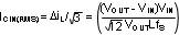
The input capacitor should be capable of handling the rms current. Although the input capacitor is not as critical in a boost application, low values can cause impedance interactions. Therefore a good quality capacitor should be chosen in the range of 100 µF to 200 µF. If a value lower than 100 µF is used, then problems with impedance interactions or switching noise can affect the LM3481-Q1 . To improve performance, especially with VIN below 8 V, it is recommended to use a 20Ω resistor at the input to provide a RC filter. This resistor is placed in series with the VIN pin with only a bypass capacitor attached to the VIN pin directly (see Figure 7-5). A 0.1-µF or 1-µF ceramic capacitor is necessary in this configuration. The bulk input capacitor and inductor will connect on the other side of the resistor with the input power supply.
 Figure 7-5 Reducing IC Input Noise