SNVSCL9 March 2011 – November 2023 LM3481-Q1
PRODUCTION DATA
- 1
- 1 Features
- 2 Applications
- 3 Description
- 4 Pin Configuration and Functions
- 5 Specifications
- 6 Detailed Description
-
7 Application and Implementation
- 7.1 Application Information
- 7.2
Typical Applications
- 7.2.1
Boost Converter
- 7.2.1.1 Design Requirements
- 7.2.1.2
Detailed Design Procedure
- 7.2.1.2.1 Custom Design with WEBENCH Tools
- 7.2.1.2.2 Power Inductor Selection
- 7.2.1.2.3 Programming the Output Voltage and Output Current
- 7.2.1.2.4 Current Limit With Additional Slope Compensation
- 7.2.1.2.5 Power Diode Selection
- 7.2.1.2.6 Power MOSFET Selection
- 7.2.1.2.7 Input Capacitor Selection
- 7.2.1.2.8 Output Capacitor Selection
- 7.2.1.2.9 Driver Supply Capacitor Selection
- 7.2.1.2.10 Compensation
- 7.2.1.3 Application Curve
- 7.2.2 Typical SEPIC Converter
- 7.2.1
Boost Converter
- 7.3 Power Supply Recommendations
- 7.4 Layout
- 8 Device and Documentation Support
- 9 Revision History
- 10Mechanical, Packaging, and Orderable Information
Package Options
Mechanical Data (Package|Pins)
- DGS|10
Thermal pad, mechanical data (Package|Pins)
Orderable Information
7.2.2 Typical SEPIC Converter
 Figure 7-7 Typical SEPIC Converter using LM3481-Q1
Because the LM3481-Q1 controls a low-side N-Channel MOSFET, it can also be used in SEPIC (Single Ended Primary Inductance Converter) applications. An example of SEPIC using the LM3481-Q1 is shown in Figure 7-7. As shown in Figure 7-7, the output voltage can be higher or lower than the input voltage. The SEPIC uses two inductors to step-up or step-down the input voltage. The inductors L1 and L2 can be two discrete inductors or two windings of a coupled transformer because equal voltages are applied across the inductor throughout the switching cycle. Using two discrete inductors allows use of catalog magnetics, as opposed to a custom transformer. The input ripple can be reduced along with size by using the coupled windings of transformer for L1 and L2.
Due to the presence of the inductor L1 at the input, the SEPIC inherits all the benefits of a boost converter. One main advantage of SEPIC over a boost converter is the inherent input to output isolation. The capacitor CS isolates the input from the output and provides protection against shorted or malfunctioning load. Hence, the SEPIC is useful for replacing boost circuits when true shutdown is required. This means that the output voltage falls to 0V when the switch is turned off. In a boost converter, the output can only fall to the input voltage minus a diode drop.
The duty cycle of a SEPIC is given by:
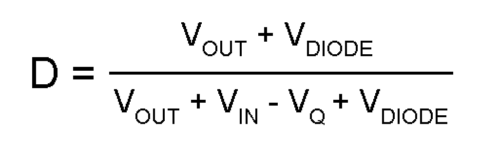
In Equation 43, VQ is the on-state voltage of the MOSFET, Q1, and VDIODE is the forward voltage drop of the diode.